
Differential amplifier and low drop-out regulator with thereof

a technology of differential amplifiers and regulators, applied in the direction of electric variable regulation, process and machine control, instruments, etc., can solve the problems of difficult operation under a small current environment, significant influence on system stability, and extremely restricted application of ldo regulators b>100/b>, and achieve the effect of a larger range of output curren

Active Publication Date: 2007-02-06
MICROCHIP TECH INC
View PDF4 Cites 25 Cited by
  • Summary
  • Abstract
  • Description
  • Claims
  • Application Information

AI Technical Summary

Benefits of technology

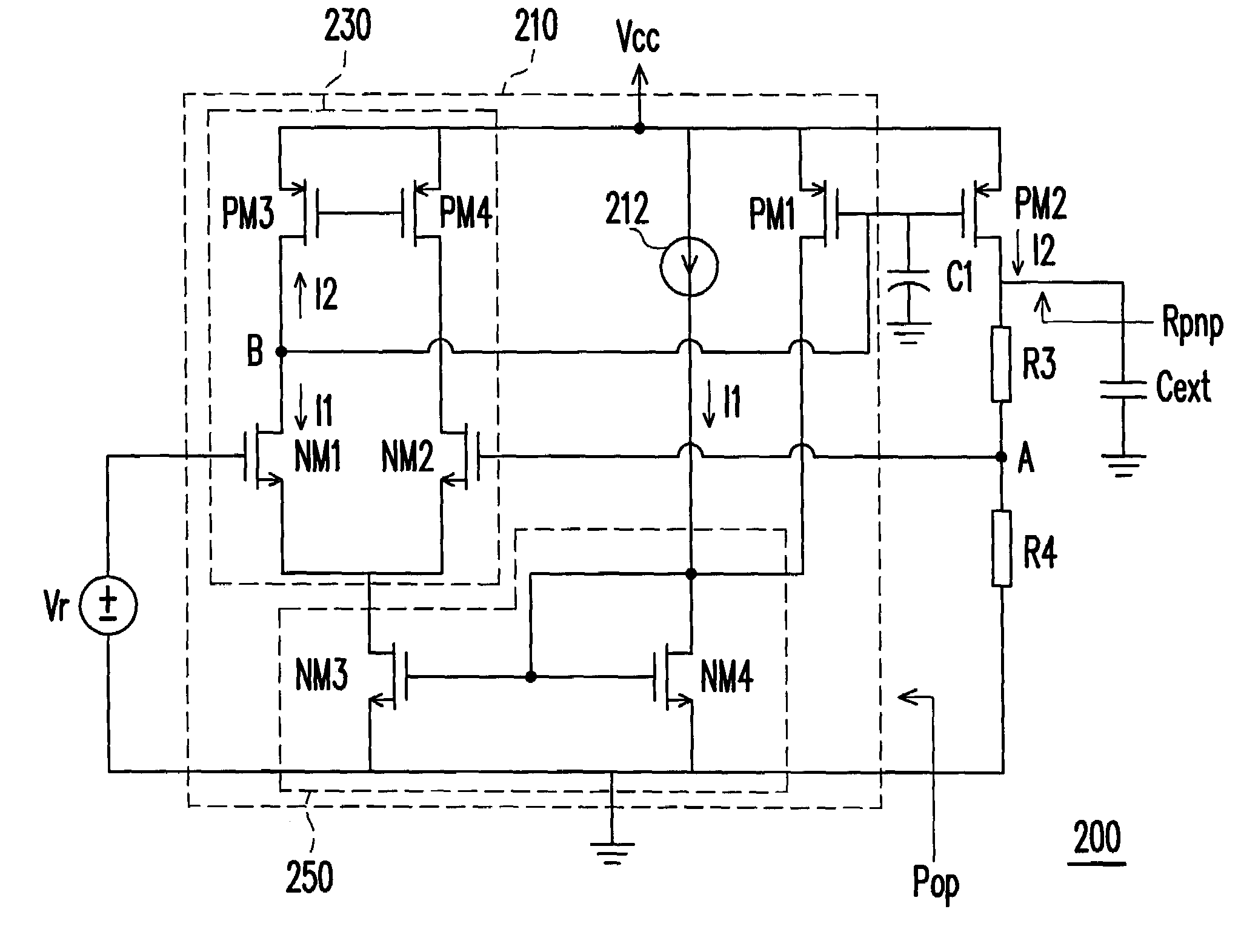
The present invention provides a differential amplifier with increased output resistance as the output current increases, which allows the non-dominant pole to move toward the high frequency zone. Additionally, the invention provides a low drop-out regulator that can provide a larger range of output current. The low drop-out regulator includes a differential amplifier with a positive input terminal, negative input terminal, output terminal, bias terminal, and ground terminal. The differential amplifier is composed of a differential pair circuit and a current mirror circuit. The current mirror circuit receives a constant current from a current source and mirrors it to the differential pair circuit, which connects to the output terminal of the differential amplifier. The output terminal of the differential amplifier connects to a second PMOS transistor, which in turn connects to the positive bias and the output terminal of the differential amplifier. The first source / drain terminal of the first PMOS transistor is grounded through a passive element, and the second source / drain terminal of the second PMOS transistor is electrically coupled to the positive bias. The invention achieves increased output resistance and decreased non-dominant pole, which results in a wider range of output current.

Problems solved by technology

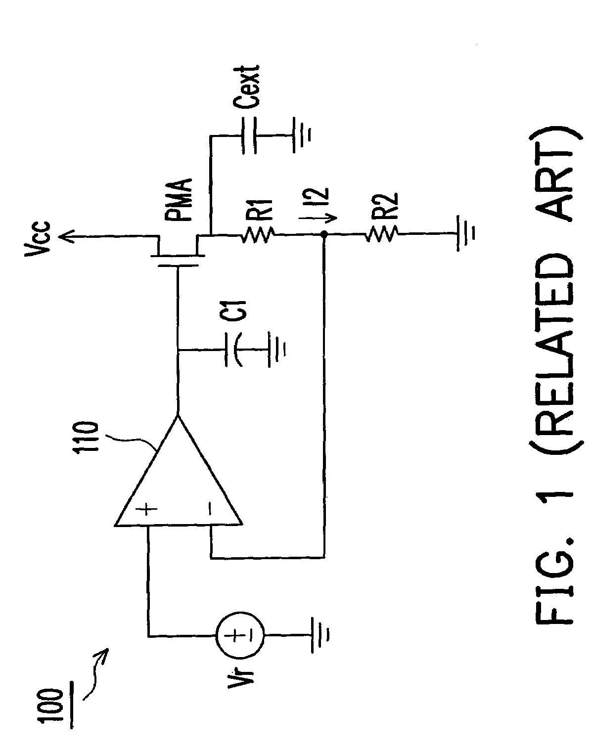
Meanwhile, the phase margin of the LDO regulator 100 may be too small, thus the system stability is significantly impacted.
Consequently, the application of the LDO regulator 100 is extremely restricted.
However, since it is required to dispose a source follower between the operational differential amplifier and the load in U.S. Pat. No. 6,188,211, although it resolves the problem of system instability under large current operation, it is not easy to operate under a small current environment.

Method used


Image

  • Differential amplifier and low drop-out regulator with thereof
  • Differential amplifier and low drop-out regulator with thereof
  • Differential amplifier and low drop-out regulator with thereof

Examples


Embodiment Construction

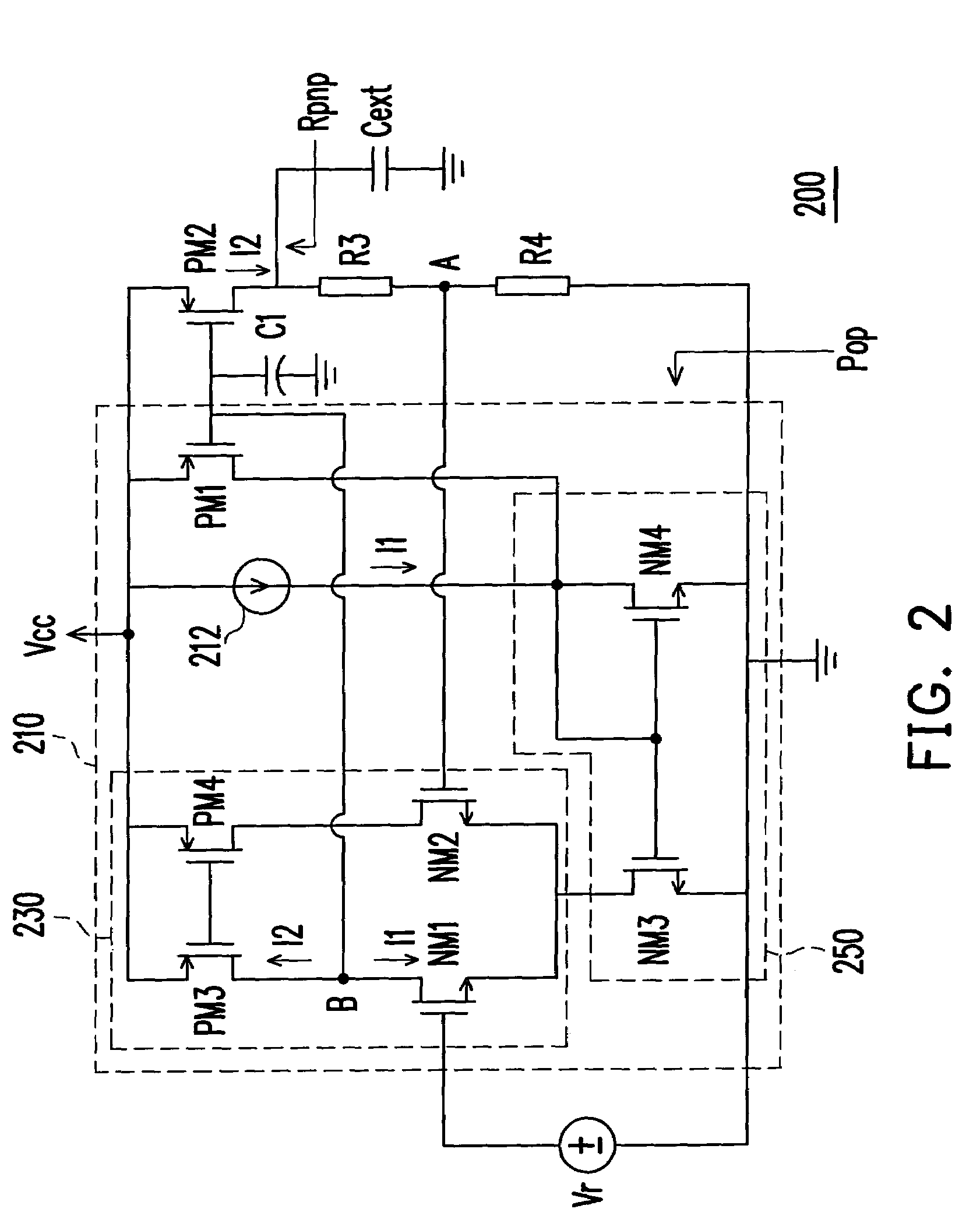
[0016]FIG. 2 schematically shows a circuit diagram of a low drop-out regulator according to a preferred embodiment of the present invention. Referring to FIG. 2, in the low drop-out regulator 200, the differential amplifier circuit 210 has a positive input terminal, a negative input terminal, an output terminal, a bias terminal and a ground terminal. Wherein, the bias terminal of the differential amplifier circuit 210 is electrically coupled to a positive bias Vcc, and its ground terminal is grounded. The output terminal of the differential amplifier circuit 210 is electrically coupled to a gate of a PMOS transistor PM2; a first source / drain terminal of the PMOS transistor PM2 serially connects to the passive elements such as the resistors R3 and R4, and its second source / drain terminal is electrically coupled to the positive bias Vcc. As shown in FIG. 2, a first terminal of the resistor R3 is electrically coupled to the first source / drain terminal of the PMOS transistor PM2, and it...


PUM


Abstract

A differential amplifier having a positive input terminal, a negative input terminal, an output terminal, a bias terminal and a ground terminal is provided. The differential amplifier comprises a differential pair circuit and a current mirror circuit. Wherein, the differential pair circuit is coupled to the positive input terminal, the negative input terminal, the output terminal, and the bias terminal of the differential amplifier. The current mirror circuit receives a constant current from a current source, and mirrors the constant current to the differential pair circuit. The current mirror circuit further connects to the ground terminal of the differential amplifier, and the terminal of the current mirror circuit receiving the constant current is coupled to a first source / drain terminal of a first PMOS transistor. A second source / drain and a gate of the first PMOS transistor are connected to the bias terminal and the output terminal of the differential amplifier, respectively.

Description

BACKGROUND OF THE INVENTION[0001]1. Field of the Invention[0002]The present invention relates to a differential amplifier, and more particularly, to a differential amplifier capable of providing a larger range of output current.[0003]2. Description of the Related Art[0004]FIG. 1 schematically shows a circuit diagram of a conventional low drop-out (LDO) regulator. Referring to FIG. 1, the LDO regulator 100 comprises a differential amplifier 110, and an output terminal of the differential amplifier 110 is electrically coupled to a gate of a PMOS transistor PMA. A first source / drain terminal of the PMOS transistor PMA is grounded through the resistors R1 and R2 that are serially connected. In addition, the first source / drain terminal of the PMOS transistor PMA is grounded through an external capacitor Cext, and a second source / drain terminal of the PMOS transistor PMA is electrically coupled to a DC bias Vcc. Moreover, a parasitic capacitor C1 is between the output terminal of the diff...

Claims


Application Information

Patent Timeline
Patent Type & Authority Patents(United States)
IPC IPC(8): G05F1/573
CPCG05F1/575
Inventor HUANG, CHUN-SHENG
Owner MICROCHIP TECH INC
Learn More