Laser ablation method for fabricating high performance organic devices

a high-performance, organic technology, applied in the field of laser ablation method of fabricating high-performance organic fets, can solve the problems of limiting the depth to which laser energy can perform useful ablation, and achieve the effect of improving resolution

Active Publication Date: 2007-02-13
GULA CONSULTING LLC
View PDF6 Cites 43 Cited by
  • Summary
  • Abstract
  • Description
  • Claims
  • Application Information

AI Technical Summary

Benefits of technology

[0013]According to the present invention, laser ablation is utilized to define the channel length of an organic transistor. In an embodiment of this invention, a substrate

Problems solved by technology

The ability of the material to absorb laser energy limits

Method used


Image

  • Laser ablation method for fabricating high performance organic devices
  • Laser ablation method for fabricating high performance organic devices
  • Laser ablation method for fabricating high performance organic devices

Examples


Embodiment Construction

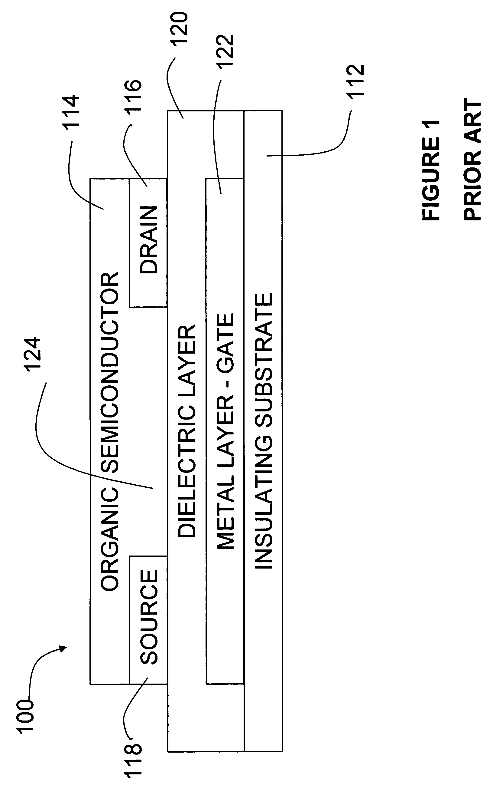
[0026]Referring to FIG. 4, a system for laser ablation of a metal layer of a top gate organic transistor is shown. The light from an excimer laser 401 is appropriately blocked by photomask 402, and impacts the metal layer 403 on insulating substrate 404 where there is an opening in the photomask 402. The light energy is of appropriate wavelength, absorption depth, pulse width, and repetition rate as to vaporize the metal where the light impacts on the metal. Laser ablation can typically ablate line width of 10 μm and higher. In one embodiment of this invention, the metal layer 404 is made unusually thin, 20 nm to 60 nm, in order to attain a capability to ablate much finer lines, in the order of 2 μm to 4 μm.

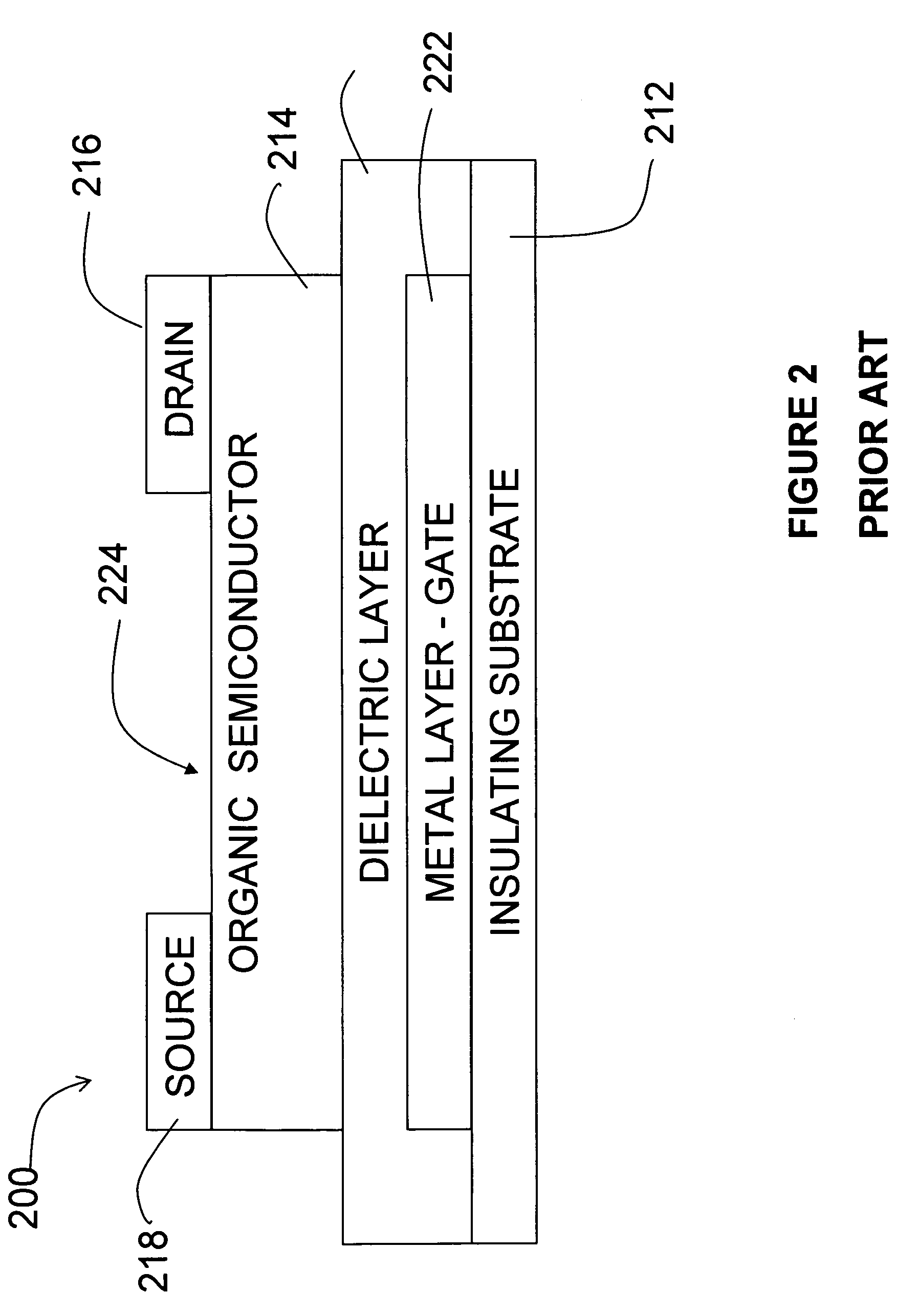
[0027]FIG. 5 shows the same system described above when applied to the definition of the channel on a bottom gate, bottom contact device. In this case, the metal layer 518 being ablated is on top of dielectric layer 520.

[0028]FIG. 6 shows the same system described above when appl...


PUM


Abstract

A laser ablation method is utilized to define the channel length of an organic transistor. A substrate is coated with a deposition of a metal or conductive polymer deposition, applied in a thin layer in order to enhance the resolution that can be attained by laser ablation. The laser ablation method can be used in a roll-to-roll process, and achieves speeds, volumes, prices and resolutions that are adequate to produce printed electronic technologies.

Description

BACKGROUND[0001]1. Field of Invention[0002]The present invention relates to organic transistors and, more particularly, to a laser ablation method of fabricating high performing organic FETs utilizing an efficient high volume patterning technique to define the channel length.[0003]2. Description of Related Art[0004]Organic MOS transistors are similar to silicon metal-oxide-semiconductor transistors in operation. The major difference in construction is that the organic MOS transistor utilizes a thin layer of a semiconducting organic polymer film to act as the semiconductor of the device, as opposed to a silicon layer as used in the more typical in-organic silicon MOS device.[0005]Referring now to FIG. 1, a cross-sectional diagram of a bottom-gate bottom-contact organic MOS transistor 100 is shown. A metallic region 122 is deposited on an insulating substrate 112 forming the gate 122 of the organic MOS device 100. A thin dielectric region 120 is placed on top of gate region 122 to ele...

Claims


Application Information

Patent Timeline
IPC IPC(8): H01L51/40
CPCB82Y30/00H01L51/102H01L51/0023H01L27/283H01L51/0541H01L51/0545H10K19/10H10K71/621H10K10/464H10K10/466H10K10/82H10K10/46
Inventor DIMMLER, KLAUS
Owner GULA CONSULTING LLC
Why Eureka
Try Eureka