Method for making a semiconductor device that includes a metal gate electrode

a metal gate electrode and semiconductor technology, applied in the direction of semiconductor devices, basic electric elements, electrical equipment, etc., can solve the problems of failure success in doing so, and inability to form extremely thin etched polysilicon

Inactive Publication Date: 2007-02-13
INTEL CORP
View PDF48 Cites 59 Cited by
  • Summary
  • Abstract
  • Description
  • Claims
  • Application Information

AI Technical Summary

Problems solved by technology

It may not be possible, however, to form an etched polysilicon layer with a width of about 45 nm (or less) that is suitable for high volume manufacturing using conventional photolithographic techniques.
While it may be difficult to form extremely thin etched polysilicon layers, any success in doing so may raise another problem—if those patterned polysilicon layers have substantially vertical side walls.
After removing such a patterned polysilicon layer, it may be difficult to uniformly coat the sidewalls of the resulting trench with various materials.
In addition, it may not be possible to completely fill such a trench with metal, as voids may form at the trench center.

Method used


Image

  • Method for making a semiconductor device that includes a metal gate electrode
  • Method for making a semiconductor device that includes a metal gate electrode
  • Method for making a semiconductor device that includes a metal gate electrode

Examples


Embodiment Construction

[0008]A method for making a semiconductor device is described. That method comprises forming a dielectric layer on a substrate, then forming on the dielectric layer a sacrificial structure that comprises a first layer and a second layer such that the second layer is wider than the first layer. After removing the sacrificial structure to generate a trench, a metal gate electrode is formed within the trench.

[0009]In the following description, a number of details are set forth to provide a thorough understanding of the present invention. It will be apparent to those skilled in the art, however, that the invention may be practiced in many ways other than those expressly described here. The invention is thus not limited by the specific details disclosed below.

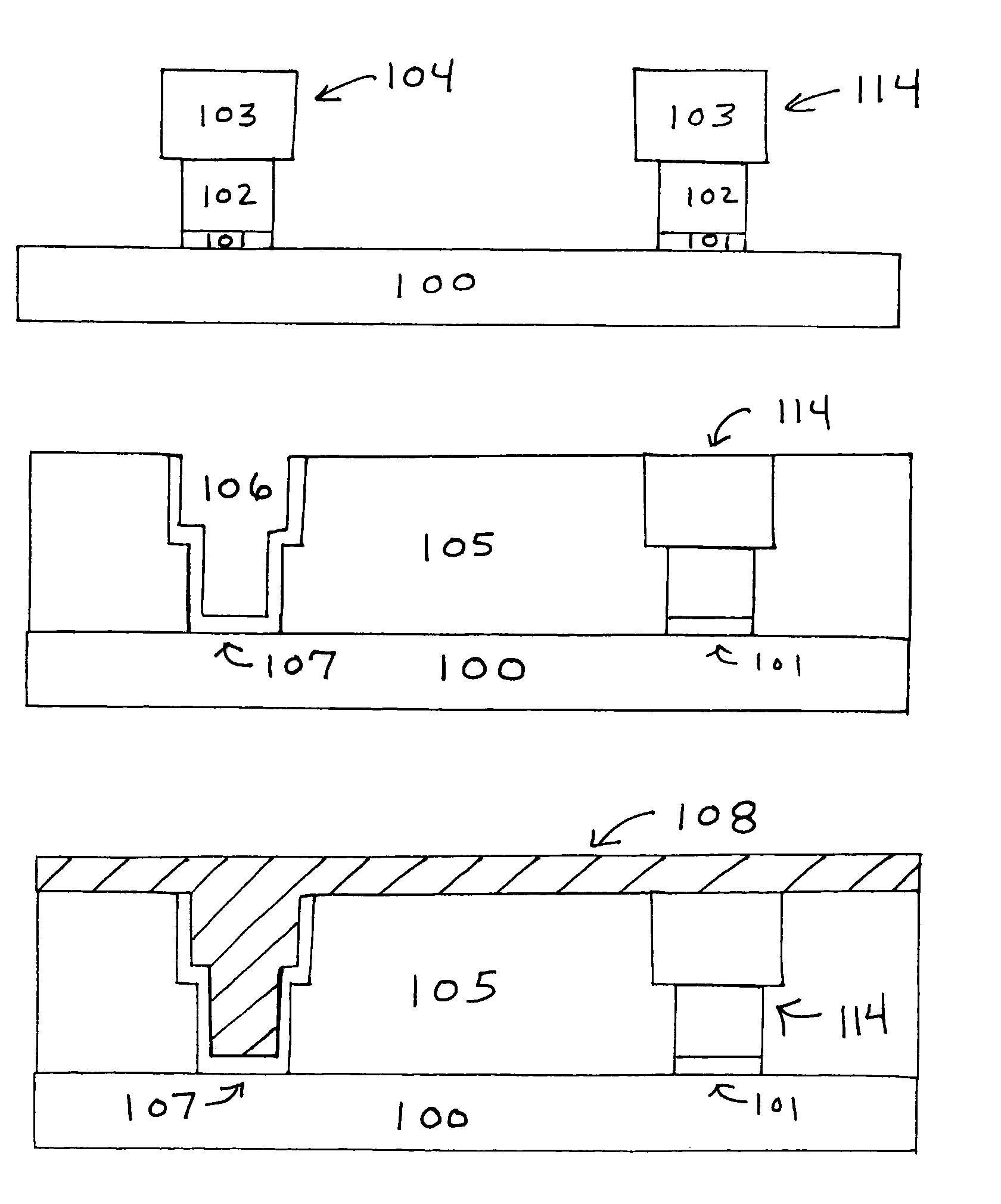
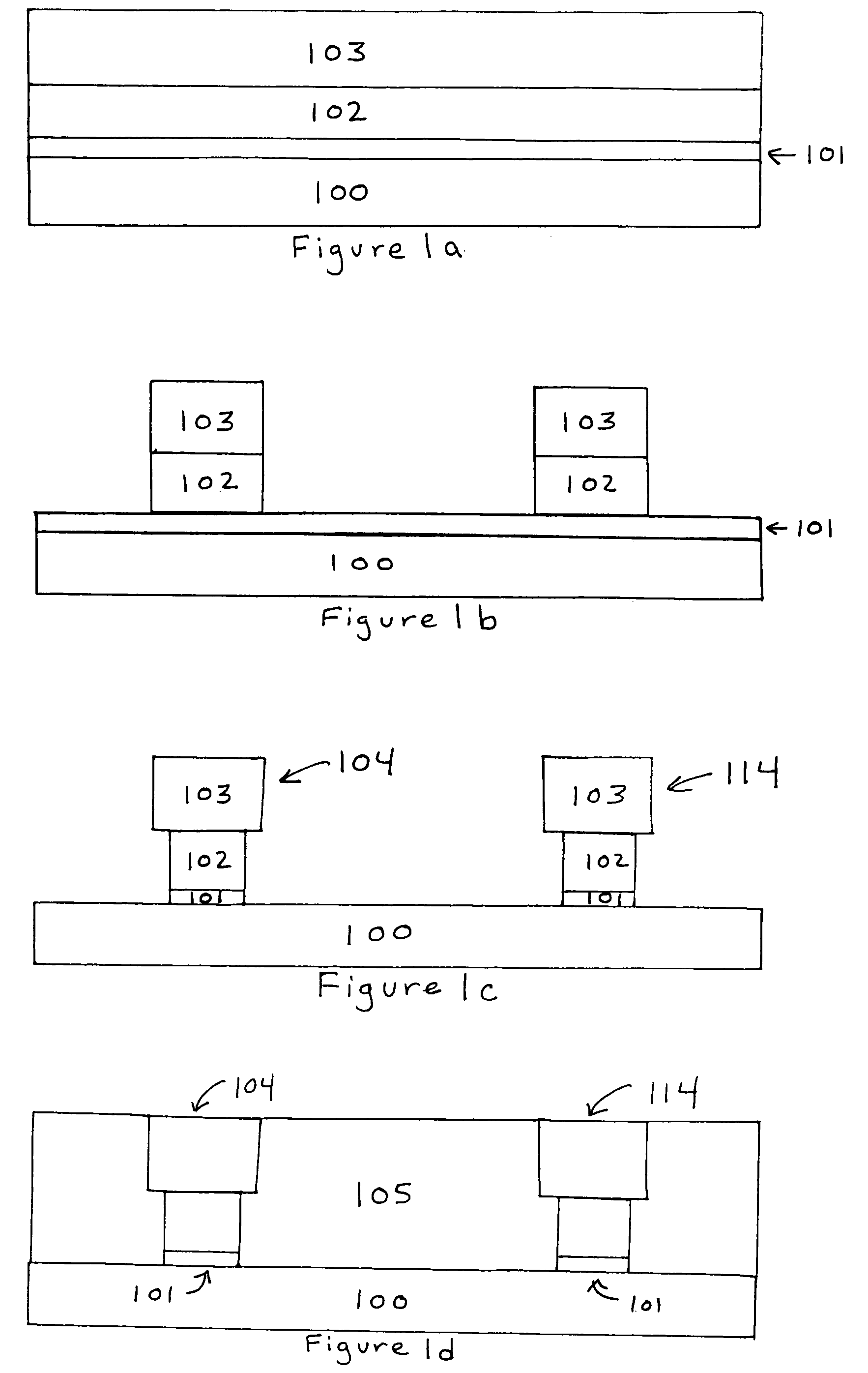
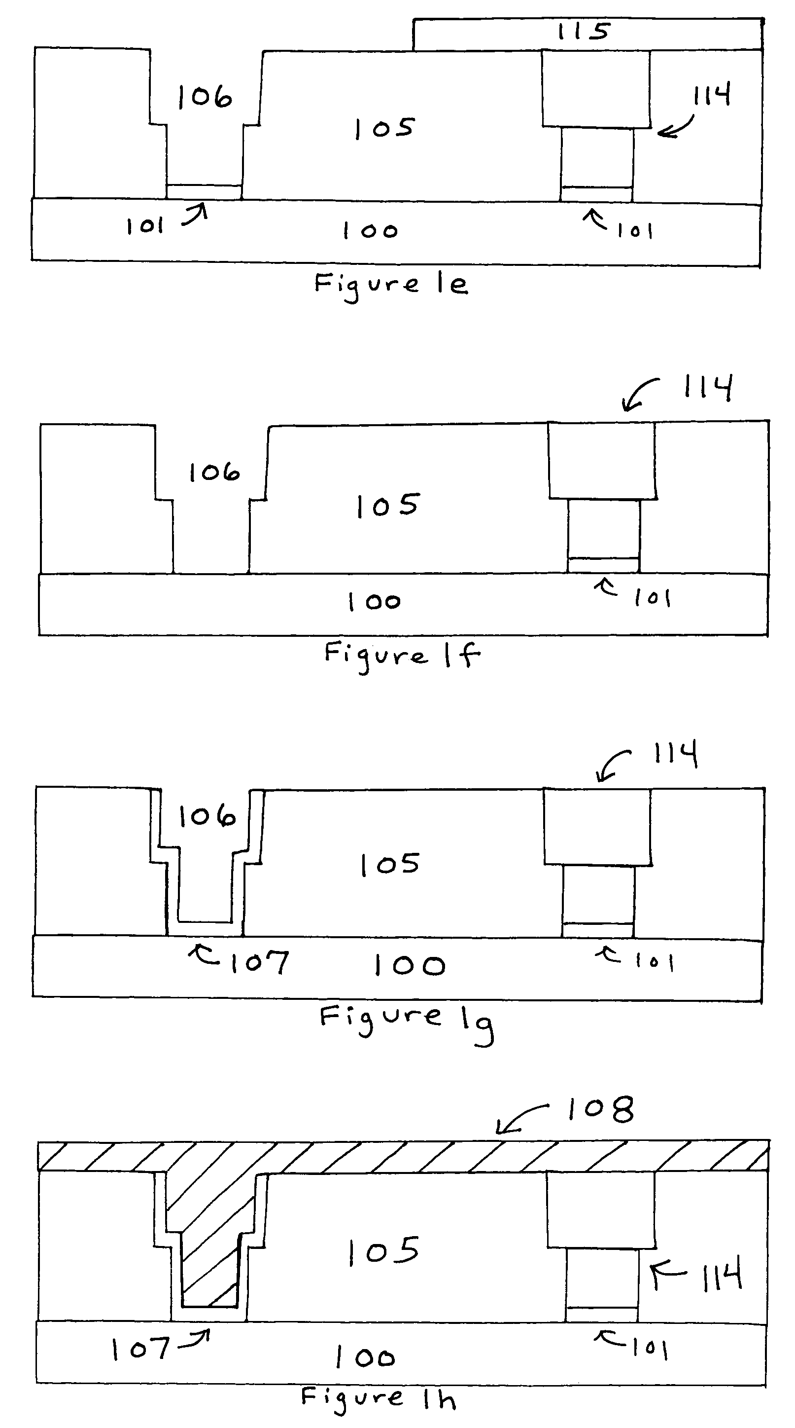
[0010]FIGS. 1a–1l represent cross-sections of structures that may be formed, when carrying out an embodiment of the method of the present invention. Initially, first dielectric layer 101 is formed on substrate 100, first layer 102 i...


PUM

PropertyMeasurementUnit
thickaaaaaaaaaa
thickaaaaaaaaaa
thickaaaaaaaaaa

Abstract

A method for making a semiconductor device is described. That method comprises forming on a substrate a dielectric layer and a sacrificial structure that comprises a first layer and a second layer, such that the second layer is formed on the first layer and is wider than the first layer. After the sacrificial structure is removed to generate a trench, a metal gate electrode is formed within the trench.

Description

FIELD OF THE INVENTION[0001]The present invention relates to methods for making semiconductor devices, in particular, semiconductor devices with metal gate electrodes.BACKGROUND OF THE INVENTION[0002]When making a CMOS device that includes metal gate electrodes, a replacement gate process may be used to form gate electrodes from different metals. In that process, a first polysilicon layer, bracketed by a pair of spacers, is removed to create a trench between the spacers. The trench is filled with a first metal. A second polysilicon layer is then removed, and replaced with a second metal that differs from the first metal.[0003]In such a replacement gate process, the first and second polysilicon layers (to be replaced with metal) are etched polysilicon layers that define the gate lengths for the subsequently formed metal gate electrodes. In a particular application, it may be desirable to create metal gate electrodes with 45 nm (or shorter) gate lengths. It may not be possible, howeve...

Claims


Application Information

Patent Timeline
Patent Type & Authority Patents(United States)
IPC IPC(8): H01L21/336
CPCH01L21/28114H01L21/823828H01L29/42376H01L29/66545H01L21/82385H01L21/30608Y10S438/926H01L21/18H01L21/28H01L21/8238H01L29/423
Inventor BRASK, JUSTIN K.KAVALIEROS, JACKDOCZY, MARK L.METZ, MATTHEW V.DATTA, SUMANSHAH, UDAYDOYLE, BRIAN S.CHAU, ROBERT S.
Owner INTEL CORP
Why Eureka
Try Eureka