Method for depinning the Fermi level of a semiconductor at an electrical junction and devices incorporating such junctions

a technology of fermi level and semiconductor, applied in the direction of semiconductor devices, electrical apparatus, radio frequency controlled devices, etc., can solve the problems that bardeen's model (like schottky's) is best considered as a limiting case, and no one explanation satisfies all experimental observations regarding such junctions

Inactive Publication Date: 2007-02-13
ACORN SEMI LLC
View PDF36 Cites 69 Cited by
  • Summary
  • Abstract
  • Description
  • Claims
  • Application Information

AI Technical Summary

Benefits of technology

[0018]A further embodiment of the present invention provides for depinning the Fermi level of a semiconductor in an electrical junction through the use of an interface layer disposed between a surface of the semiconductor and a conductor. The interface layer preferably (i) is of a thickness sufficient to reduce effects of MIGS in the semiconductor, and (ii) passivates the surface of the semiconductor. Despite the presence of the interface layer, significant current may flow between the conductor and the semiconductor because the thickness of the interface layer may be chosen to provide a minimum (or near minimum) specific contact resistance for the junction. As indicated above, the interface layer may include a passivating material such as a nitride, oxide, oxynitride, arsenide, hydride and / or fluoride.

Problems solved by technology

This condition is rarely observed experimentally, however, and so Bardeen's model (like Schottky's) is best considered as a limiting case.
Indeed, to this day no one explanation satisfies all experimental observations regarding such junctions.

Method used


Image

  • Method for depinning the Fermi level of a semiconductor at an electrical junction and devices incorporating such junctions
  • Method for depinning the Fermi level of a semiconductor at an electrical junction and devices incorporating such junctions
  • Method for depinning the Fermi level of a semiconductor at an electrical junction and devices incorporating such junctions

Examples


Embodiment Construction

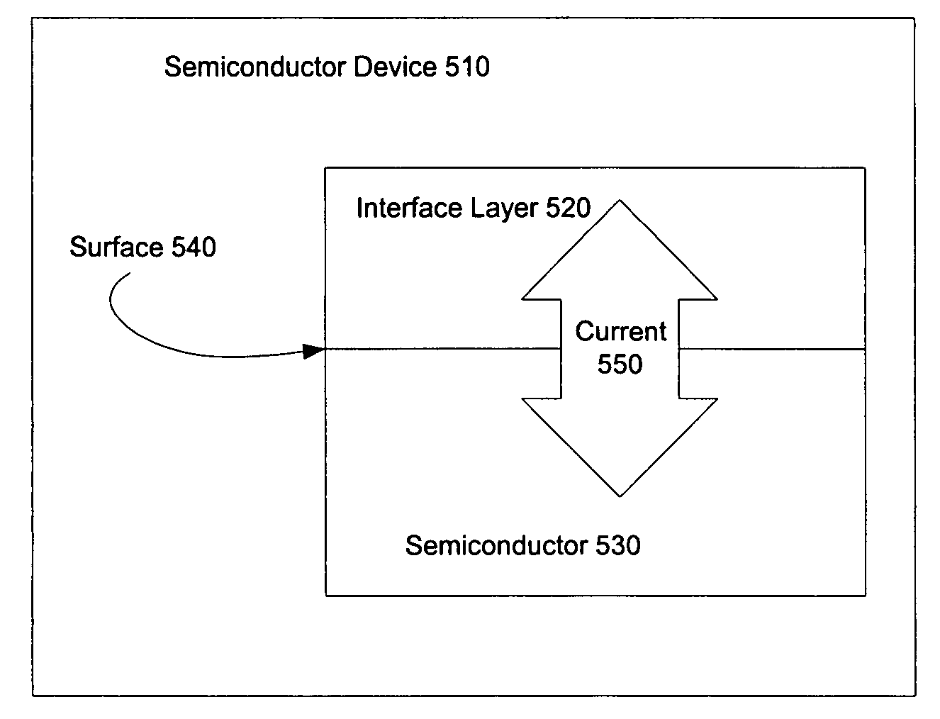
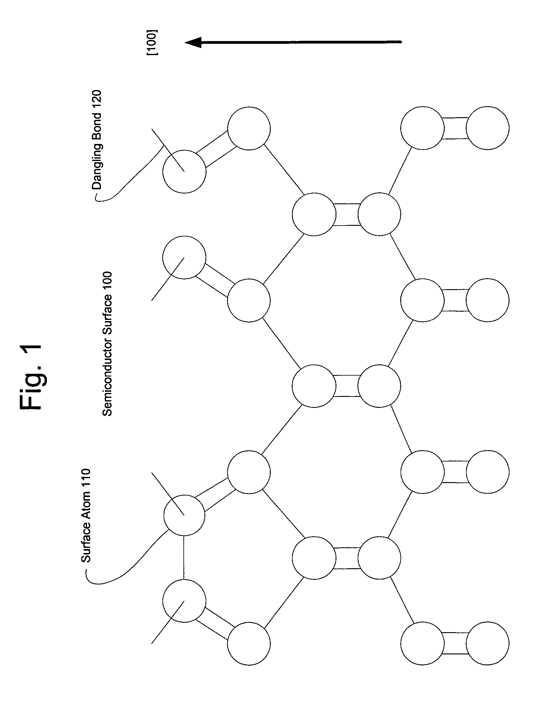
[0029]Described herein are processes for depinning the Fermi level of a semiconductor (e.g., Si, Ge, C (the crystal structure of which may be either a diamond lattice, or another bonding scheme such as a fulleride (an example of which are carbon nanotubes) or polymer), an alloy of Ge and Si, an alloy of Ge and C, an alloy of Si and C, or an alloy of Si, Ge, and C) at a metal-semiconductor junction as well as devices that use such a junction. As more fully discussed below, an interface layer is introduced between the semiconductor and the metal. The interface layer functions to passivate the semiconductor surface (that is, terminate dangling bonds that may otherwise be present at the semiconductor surface so as to assure chemical stability of the surface) and to displace the semiconductor from the metal so as to reduce the effect of MIGS.

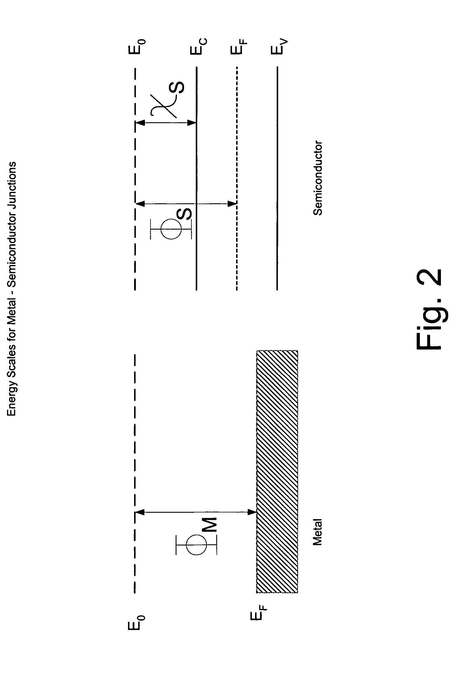
[0030]As discussed more fully below, the present inventors have determined that for thin interface layers disposed between a metal and a semiconduct...


PUM

PropertyMeasurementUnit
energy gapaaaaaaaaaa
thicknessaaaaaaaaaa

Abstract

An electrical junction that includes a semiconductor (e.g., C, Ge, or an Si-based semiconductor), a conductor, and an interface layer disposed therebetween. The interface layer is sufficiently thick to depin a Fermi level of the semiconductor, yet sufficiently thin to provide the junction with a specific contact resistance of less than or equal to approximately 1000 Ω-μm2, and in some cases a minimum specific contact resistance.

Description

RELATED APPLICATIONS[0001]The present application is a Continuation-in-Part of application Ser. No. 10 / 217,758, (U.S. Pat. No. 7,084,423) entitled “Method for Depinning the Fermi Level of a Semiconductor at an Electrical Junction and Devices Incorporating Such Junctions”, filed Aug. 12, 2002 and is also related to U.S. patent application Ser. No. 10 / 342,576, (U.S. Pat. No. 6,833,556) entitled “Insulated Gate Field effect Transistor Having Passivated Schottky Barriers to the Channel”, filed on Jan. 14, 2003, both by the present inventors and assigned to the same assignee as the present application. These related patent applications are hereby incorporated by reference in their entireties.FIELD OF THE INVENTION[0002]The invention relates generally to semiconductor processing and semiconductor devices. More particularly, the invention relates to a process for depinning the Fermi level of a semiconductor at a metal-interface layer-semiconductor junction and to devices that employ such a...

Claims


Application Information

Patent Timeline
Patent Type & Authority Patents(United States)
IPC IPC(8): H01L39/00H01L21/285H01L21/329H01L21/336H01L29/08H01L29/45H01L29/47H01L29/78H01L29/786H01L29/812H01L29/872
CPCH01L21/28537H01L29/0895H01L29/45H01L29/456H01L29/47H01L29/812H01L29/66636H01L29/7827H01L29/7839H01L29/66143H01L29/78H01L29/785
Inventor GRUPP, DANIEL E.CONNELLY, DANIEL J.
Owner ACORN SEMI LLC
Why Eureka
Try Eureka