
Block redundancy implementation in heirarchical RAM'S
a technology of block redundancy and block redundancy, applied in the field of programable devices, can solve the problems of high-performance memory architectures that place a severe strain on the power and area budgets of the associated systems, require complex fabrication and manufacturing processes, and require high-performance components such as memory cells. to achieve the effect of not incurring excessive access time or area overhead penalties
- Summary
- Abstract
- Description
- Claims
- Application Information
AI Technical Summary
Benefits of technology
Problems solved by technology
Method used
Image

Examples
Embodiment Construction
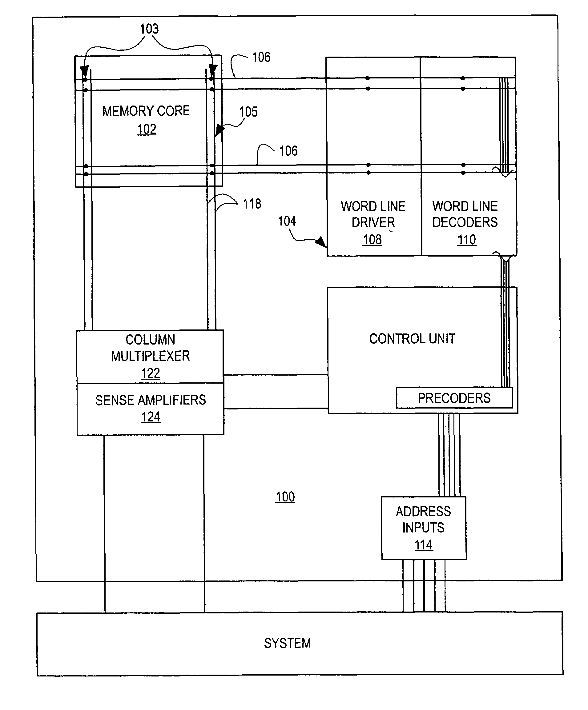
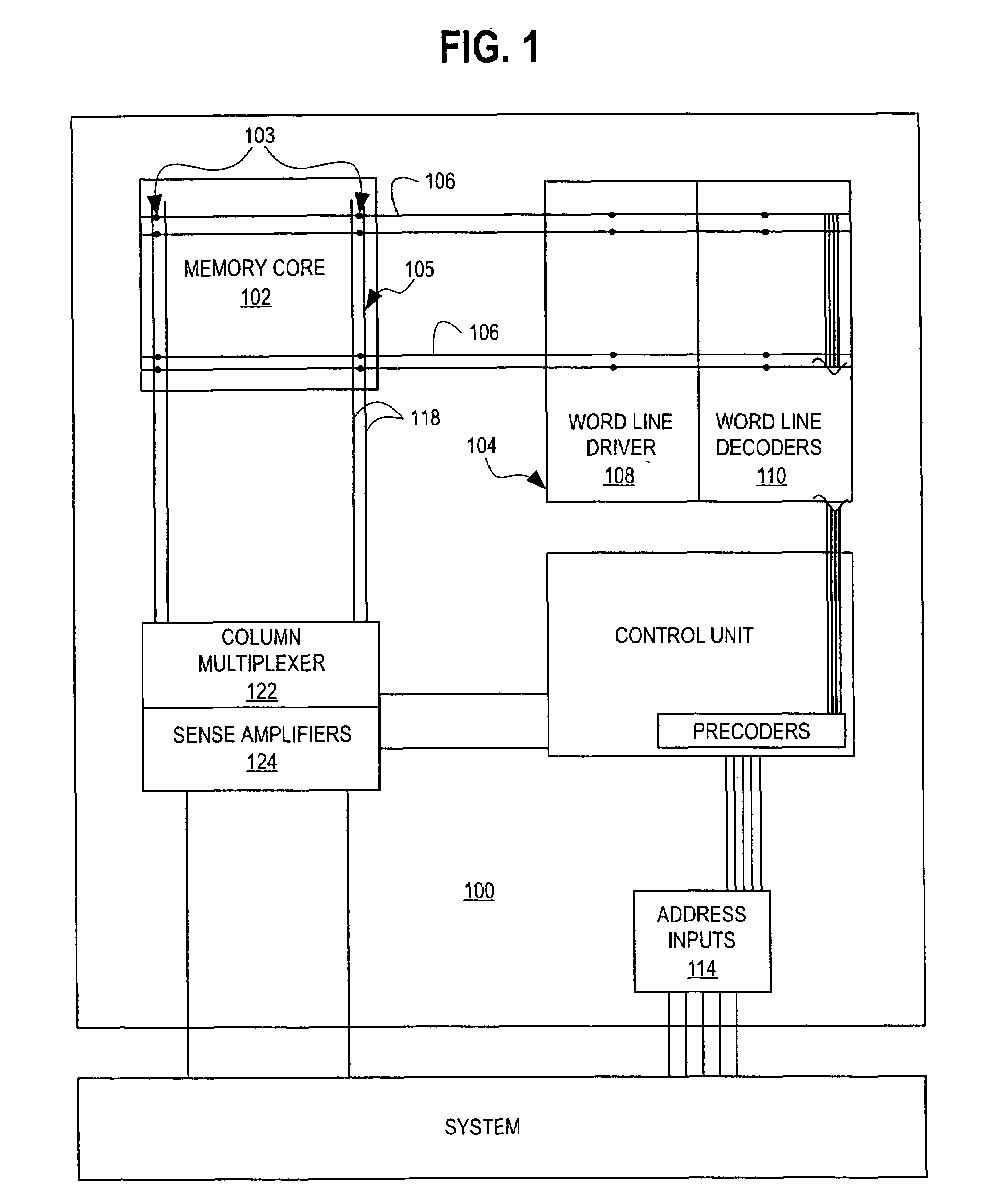
[0057]As will be understood by one skilled in the art, most VLSI systems, including communications systems and DSP devices, contain VLSI memory subsystems. Modern applications of VLSI memory subsystems almost invariably demand high efficiency, high performance implementations that magnify the design tradeoffs between layout efficiency, speed, power consumption, scalability, design tolerances, and the like. The present invention ameliorates these tradeoffs using a novel synchronous, self-timed hierarchical architecture. The memory module of the present invention also may employ one or more novel components, which further add to the memory module's efficiency and robustness.
[0058]It should be appreciated that it is useful to describe the various aspects and embodiments of the invention herein in the context of an SRAM memory structure, using CMOS SRAM memory cells. However, it should be further appreciated by those skilled in the art the present invention is not limited to CMOS-based ...
PUM
 Abstract
Description
Claims
Application Information