Method of forming an integrated circuit having nanocluster devices and non-nanocluster devices

a technology of nanoclusters and integrated circuits, applied in the field of semiconductor devices having nanoclusters, can solve the problems of nanocluster oxidation, damage to memory, and unfavorable increase of nanocluster-based memory bottom dielectric thickness

Inactive Publication Date: 2007-02-27
NORTH STAR INNOVATIONS
View PDF11 Cites 41 Cited by
  • Summary
  • Abstract
  • Description
  • Claims
  • Application Information

AI Technical Summary

Problems solved by technology

When nanocluster-based memories are integrated with transistors having thick gate oxide layers for handling relatively higher voltages and with transistors having thinner gate oxide layers, the severe oxidizing ambient used to make such transistors causes an undesirable increase in the nanocluster-based memory bottom dielectric thickness and also causes nanocluster oxidation.
Any protection layer that is used to protect nanocluster-based memories may result in damage to the memories when the protection layer is removed.

Method used


Image

  • Method of forming an integrated circuit having nanocluster devices and non-nanocluster devices
  • Method of forming an integrated circuit having nanocluster devices and non-nanocluster devices
  • Method of forming an integrated circuit having nanocluster devices and non-nanocluster devices

Examples


Embodiment Construction

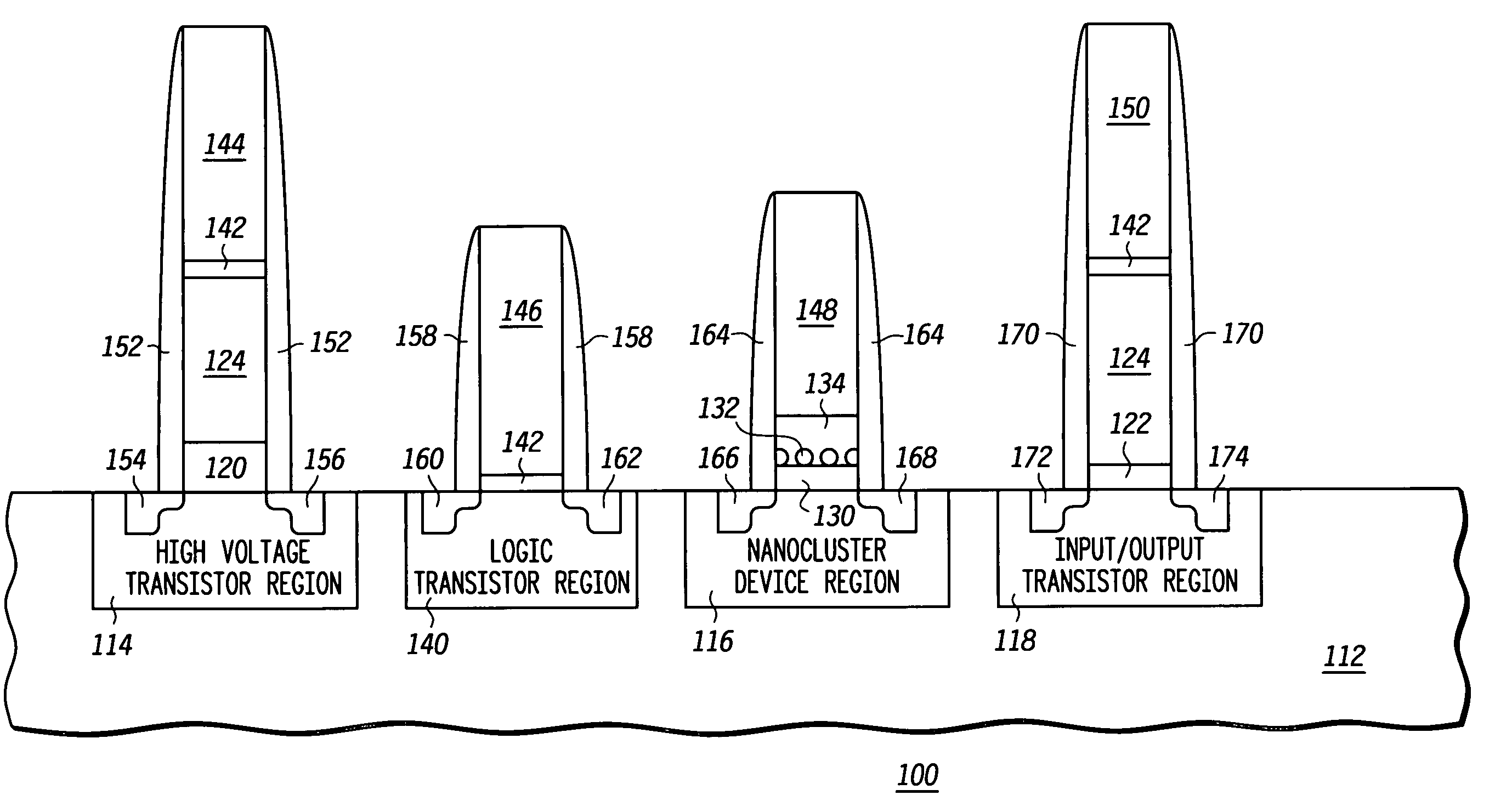
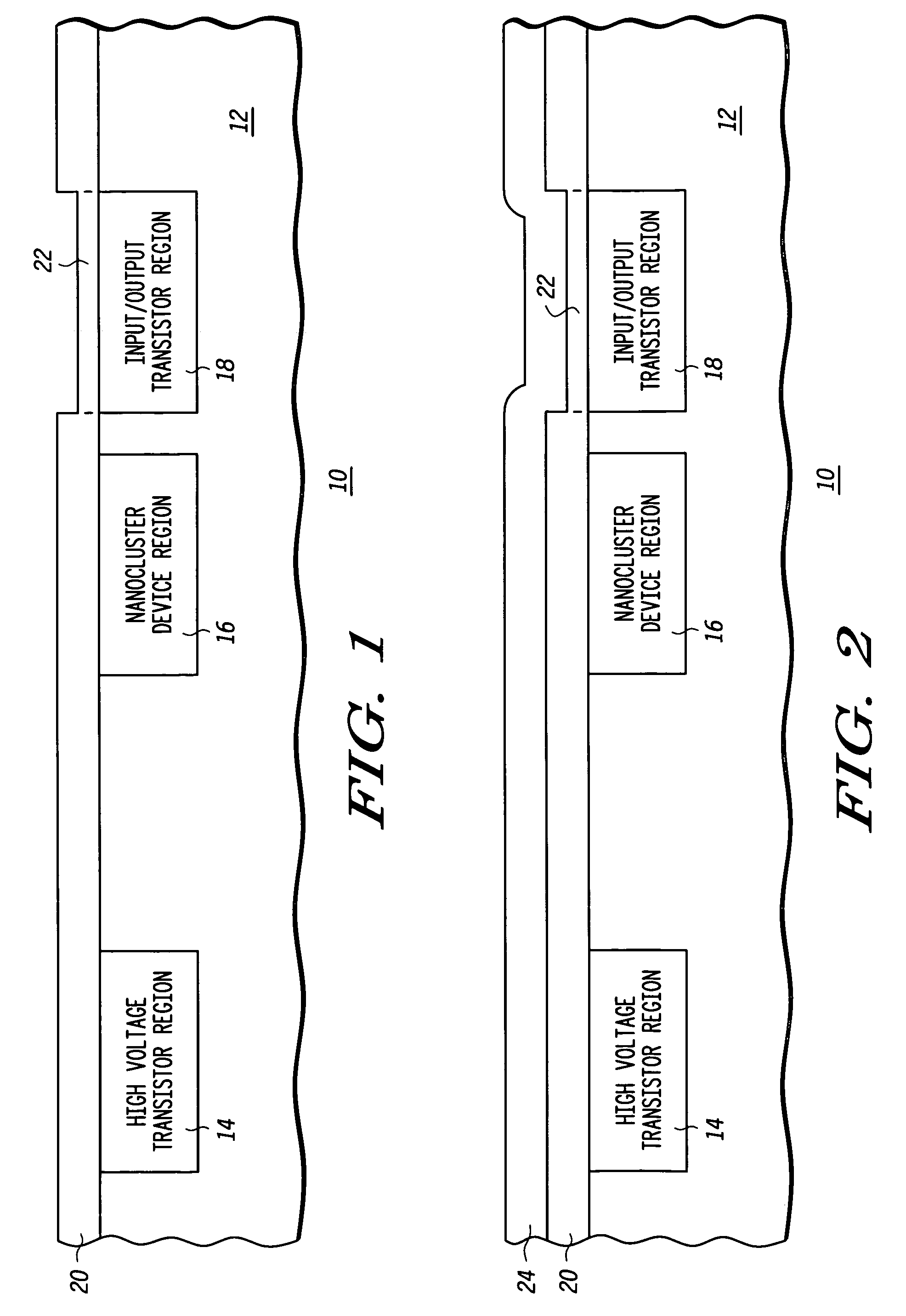
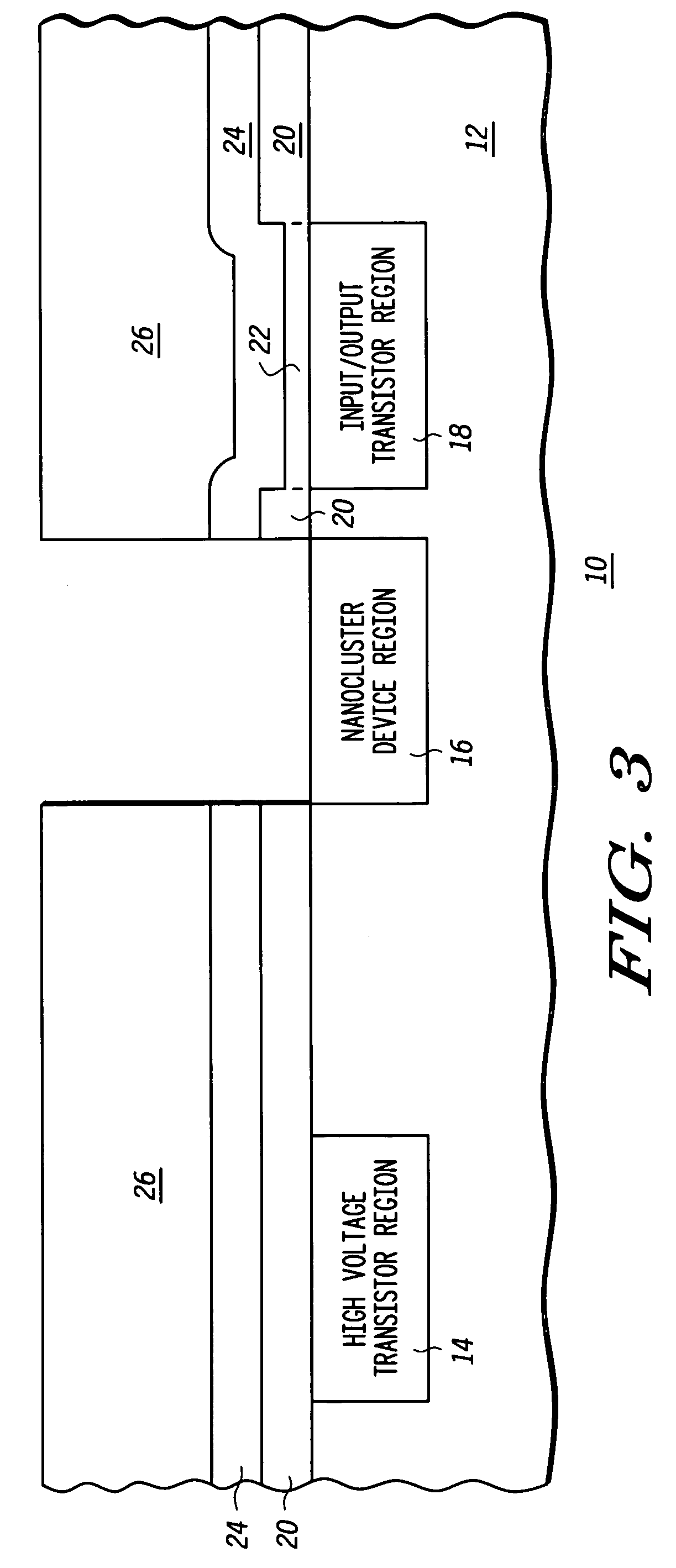
[0011]Illustrated in FIG. 1 is an integrated circuit 10 having a substrate 12 that contains various regions with differing types of semiconductor devices. For example, within substrate 12 is a high voltage transistor region 14, a nanocluster device region 16 and an input / output (I / O) transistor region 18. A high voltage transistor, as used herein, is a transistor that is used to program and erase nanocluster charge storage devices or is a device that requires a high voltage (i.e. greater than six volts) operation. An I / O transistor, as used herein, is a transistor that is used to interface the electrical functions performed in the integrated circuit 10 with other components or circuitry (not shown) external to integrated circuit 10. Within each of high voltage transistor region 14, nanocluster device region 16 and the I / O transistor region 18 will be formed a plurality of semiconductor structures to be described below. For drawing simplicity, a single device is illustrated in each o...


PUM


Abstract

An integrated circuit is formed by identifying multiple regions, each having transistors that have a gate oxide thickness that differs between the multiple regions. One of the regions includes transistors having a nanocluster layer and another of the regions includes transistors with a thin gate oxide used for logic functions. Formation of the gate oxides of the transistors is sequenced based upon the gate oxide thickness and function of the transistors. Thin gate oxides for at least one region of transistors are formed after the formation of gate oxides for the region including the transistors having the nanocluster layer.

Description

CROSS REFERENCE TO RELATED APPLICATIONS[0001]This application is related to the following pending applications:[0002](1) U.S. Ser. No. 10 / 876,805 (Robert F. Steimle) published as U.S. 2005-0287729A1 and entitled “Method of Forming a Nanocluster Charge Storage Device”, filed Jun. 24, 2004 and assigned to the assignee hereof and[0003](2) U.S. Ser. No. 10 / 663,621 (Robert F. Steimle et al.), now U.S. Pat. No. 6,958,265 entitled “Semiconductor Device With Nanoclusters”, filed Sep. 16, 2003 and assigned to the assignee hereof.FIELD OF THE INVENTION[0004]This invention relates generally to semiconductor devices, and more specifically, to making semiconductor devices having nanoclusters.BACKGROUND OF THE INVENTION[0005]Some devices such as memories (e.g. non volatile memories) utilize discrete charge storage elements called nanoclusters (e.g. of silicon, aluminum, gold, or germanium) for storing charge in a charge storage location of a transistor. In some examples, the nanoclusters are loca...

Claims


Application Information

Patent Timeline
Patent Type & Authority Patents(United States)
IPC IPC(8): H01L21/336
CPCB82Y10/00H01L21/823462H01L27/088H01L27/105H01L27/11546H01L27/11526Y10S977/774H01L29/785Y10S438/962Y10S977/943H10B41/49H10B41/40
Inventor RAO, RAJESH A.STEIMLE, ROBERT F.
Owner NORTH STAR INNOVATIONS
Why Eureka
Try Eureka