Method of making low kappa dielectric inorganic/organic hybrid films

a dielectric hybrid and organic technology, applied in the direction of resistive material coating, semiconductor/solid-state device details, superimposed coating process, etc., can solve the problems of reducing efficiency, increasing the rc delay of the circuit, and having a detrimental effect on the speed of the device, so as to achieve good thermal stability and good thermal stability

Inactive Publication Date: 2000-05-30
APPLIED MATERIALS INC
View PDF5 Cites 408 Cited by
  • Summary
  • Abstract
  • Description
  • Claims
  • Application Information

AI Technical Summary

Benefits of technology

More particularly, it is an object of the present invention to provide a dielectric film comprised of an inorganic / organic hybrid material having a low dielectric constant and good thermal stability for use in semiconductors and integrated circuits.
Another object of the present invention is to employ precursors of organosilicon, such as siloxanes, to form an inorganic / organic hybrid dielectric material having a low .kappa. and good thermal stability for use in semiconductor and / or integrated circuit applications.

Problems solved by technology

One of the greatest challenges for the microelectronics industry in the coming years is to identify advanced dielectric materials that will replace silicon dioxide as an inter and intra metal layer dielectric.
These trends increase the RC delay of the circuit.
Increased RC delay has a detrimental effect on the speed of the device, which has tremendous commercial implications.
Further, narrower line spacing results in reduced efficiency due to the impact of higher capacitive losses and greater crosstalk.
This reduced efficiency makes the device less attractive for certain applications such as battery powered computers, mobile phones, and other devices.
Issues for fluorinated amorphous carbon remain, most notably with adhesion; the thermal stability, including dimensional stability; and the integration of the films.
Despite their lower .kappa. values, these polymers are not entirely satisfactory due to processing and material limitations.
Polymers are generally thermally and dimensionally unstable at standard processing conditions of about 400.degree. to 450.degree. C.
While these materials have been considered for embedded structures, as a rule they are not suitable for full stack gap fill or damascene structures.
However, the parylenes that have been prepared to date exhibit poor thermal stability as with ppx--N; expensive as with ppx--F, or have issues with mechanical stability.
To date, advanced low .kappa. materials have not been successfully employed in the semiconductor industry.

Method used


Image

  • Method of making low kappa dielectric inorganic/organic hybrid films
  • Method of making low kappa dielectric inorganic/organic hybrid films
  • Method of making low kappa dielectric inorganic/organic hybrid films

Examples


example 1

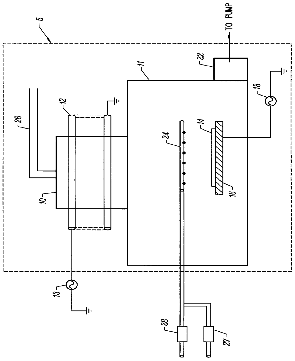
A very low .kappa. dielectric film according the present invention was formed on a 4" silicon wafer in a cylindrical plasma reactor using octamethylcyclotetrasiloxane (OMCTS) and oxygen combined in a plasma discharge generated at a frequency of 13.56 MHz. The silicon wafer was placed on a substrate holder made of copper which was electrically isolated during the deposition process. The wafer was secured onto the substrate holder with a vacuum compatible adhesive and placed into the deposition chamber. The deposition chamber was 8" in diameter and 8" in length and contains a hollow cathode electrode system which was centered to the center of the silicon wafer. The chamber was evacuated with a rotary vane pump to a pressure less than 20 mTorr. Once the chamber was evacuated, the OMCTS liquid was injected into a heated stainless steel vaporizing system which vaporized the material to form a vapor stream which was then controllably flowed into the plasma reactor at a flow rate of approx...

example 2

In a second set of experiments, low .kappa. dielectric films were deposited in accordance with another embodiment of the inventive method where the flow rate of the precursors and the plasma conditions were changed. The reactor used was identical to that described in Example 1 above and the same precursors were used, however, in this experiment the flow rate of oxygen was approximately 2.5 seem. The flow rate of OMCTS was the same at approximately 8 seem. The plasma conditions were also different, and in this case the plasma was ignited with 275 watts of power with a 13.56 MHz power supply and the plasma discharge was maintained for approximately 5 minutes. The resulting 5000 .ANG. thick film was measured with a standard aluminum dot capacitance test method and yielded a dielectric constant of 3.3. Additional films in accordance with the invention were deposited on wafers under the same conditions and procedure as outlined above, and then measured for thermal weight loss by heating ...

example 3

In a third set of experiments, very low .kappa. dielectric films were deposited in accordance with another embodiment of the present invention. In this set of experiments, a Watkins-Johnson Company HDP cluster tool reactor Model number WJ-2000H (having an inductively coupled plasma source) was used to deposit a low .kappa. film on an 8-inch silicon wafer under the following conditions: vaporized OMCTS was injected into the reactor at a liquid flow rate of 0.300 ccm (measured at room temperature). Additionally, oxygen was added at a flow rate of 20 sccm. The plasma source was operated at an RF input power of approximately 600 Watts (a power density of 1200 Watts / ft.sup.3) at a frequency of 13.56 MHz. The resulting pressure in the reactor was approximately 25 mTorr. Films were deposited under two different process times; approximately 2 minutes 45 seconds, and 6 minutes 30 seconds. The shorter process time yielded a film of approximately 5000 .ANG. thickness as measured by clipsometry...


PUM

PropertyMeasurementUnit
dielectric constantaaaaaaaaaa
power densityaaaaaaaaaa

Abstract

A method of depositing a dielectric film exhibiting a low dielectric constant in a semiconductor and/or integrated circuit by chemical vapor deposition (CVD) is provided. The film is deposited using an organosilicon precursor in a manner such that the film is comprised of a backbone made substantially of Si-O-Si or Si-N-Si groups with organic side groups attached to the backbone.

Description

This invention relates to materials having low dielectric constants. More specifically, the present invention relates to inorganic / organic hybrid films having low dielectric constant for use in semiconductors, produced using organosilicon precursors, and a method for making the same.One of the greatest challenges for the microelectronics industry in the coming years is to identify advanced dielectric materials that will replace silicon dioxide as an inter and intra metal layer dielectric. Dielectric film layers are fundamental components of integrated circuits and semiconductors. Such films provide electrical isolation between components. As device densities increase, multiple layer dielectric films are generally used to isolate device features. When forming dielectric films it is important for the film to exhibit certain properties, such as good gap fill, thermal stability and favorable electrical properties. The most widely used dielectric layer, silicon dioxide (SiO.sub.2) is for...

Claims


Application Information

Patent Timeline
Patent Type & Authority Patents(United States)
IPC IPC(8): C09D4/00C23C16/40C23C16/30H01L21/02H01L21/312B32B9/04H01L21/316H01L21/318H01L21/768H01L23/522
CPCC09D4/00C23C16/401H01L21/02126H01L21/02216H01L21/02274H01L21/3121H01L21/3122H01L21/3124H01L21/3125H01L21/31633C23C16/30C08G77/00C08G77/04Y10T428/24917Y10T428/31663Y10T428/31504B32B9/04
Inventor ROSE, PETERLOPATA, EUGENEFELTS, JOHN
Owner APPLIED MATERIALS INC
Why Eureka
Try Eureka