Integrated circuit including memory array incorporating multiple types of NAND string structures

a technology of integrated circuits and memory arrays, which is applied in the field of monolithic three-dimensional memory arrays, can solve the problems of increasing the number of devices in the memory array, increasing the number of nand string devices, and increasing the density of the memory array, so as to achieve faster read times and higher density portions

Active Publication Date: 2007-02-13
SANDISK TECH LLC
View PDF38 Cites 386 Cited by
  • Summary
  • Abstract
  • Description
  • Claims
  • Application Information

AI Technical Summary

Benefits of technology

[0012]In some embodiments, the invention provides an integrated circuit having a three-dimensional memory array that includes NAND strings having different number of memory cells in various strings. By exploiting a global bit line architecture, the read and write circuits may be shared between different types of NAND strings, thus improving the memory array efficiency. NAND strings with larger number of series devices provide a memory array having very high density, at the price of increased read and program disturb, and longer access time. In some embodiments, the longer strings may be used for data storage. NAND strings with fewer devices show improved read and program disturb, and shorter access time, and in some embodiments may be used for code or pointer storage. In addition, shorter NAND strings provide a smaller erase block size (i.e., determined by the number of series memory cells in an independently selectable NAND string), which can lead to greater flexibility for a user of such memory device. In some embodiments memory cells having a smaller erase block size may be advantageously used for pointer and file allocation table storage. In some embodiments, some or all of the array portion having shorter strings may also be used to store configuration information for internal purposes, such as redundancy information storage, thus avoiding the need for extra non-volatile bits for redundancy information. The shorter strings may be completely hidden from end user view, and may include configuration bits other than redundancy information.
[0014]In an exemplary embodiment, an integrated circuit includes a three-dimensional memory array of thin film SONOS transistor NAND strings disposed on at least two memory planes formed above a substrate, and includes a higher density portion and a lower density portion. The higher density portion may be implemented as 16T NAND strings totaling 512 Mbits, and the lower density portion implemented as 1T NAND strings totaling 4 Mbits. Both high-density and lower density portions may share global bit lines, and also may share most or all of the read / write circuits. The 1T NAND strings provide erase blocks which are 1 / 16 as large as the 16T erase blocks, provide 1 / 16 the read disturb, exhibit virtually no VPASS program disturb, and provide roughly more than 10 times the read current, as compared to the 16T blocks. This allows a higher number of reads without degradation effects and can provide faster read times.

Problems solved by technology

However, other characteristics, such as cell current, read disturb, and program disturb, may degrade with increasing number of devices in a NAND string.
NAND strings with larger number of series devices provide a memory array having very high density, at the price of increased read and program disturb, and longer access time.

Method used


Image

  • Integrated circuit including memory array incorporating multiple types of NAND string structures
  • Integrated circuit including memory array incorporating multiple types of NAND string structures
  • Integrated circuit including memory array incorporating multiple types of NAND string structures

Examples


Embodiment Construction

)

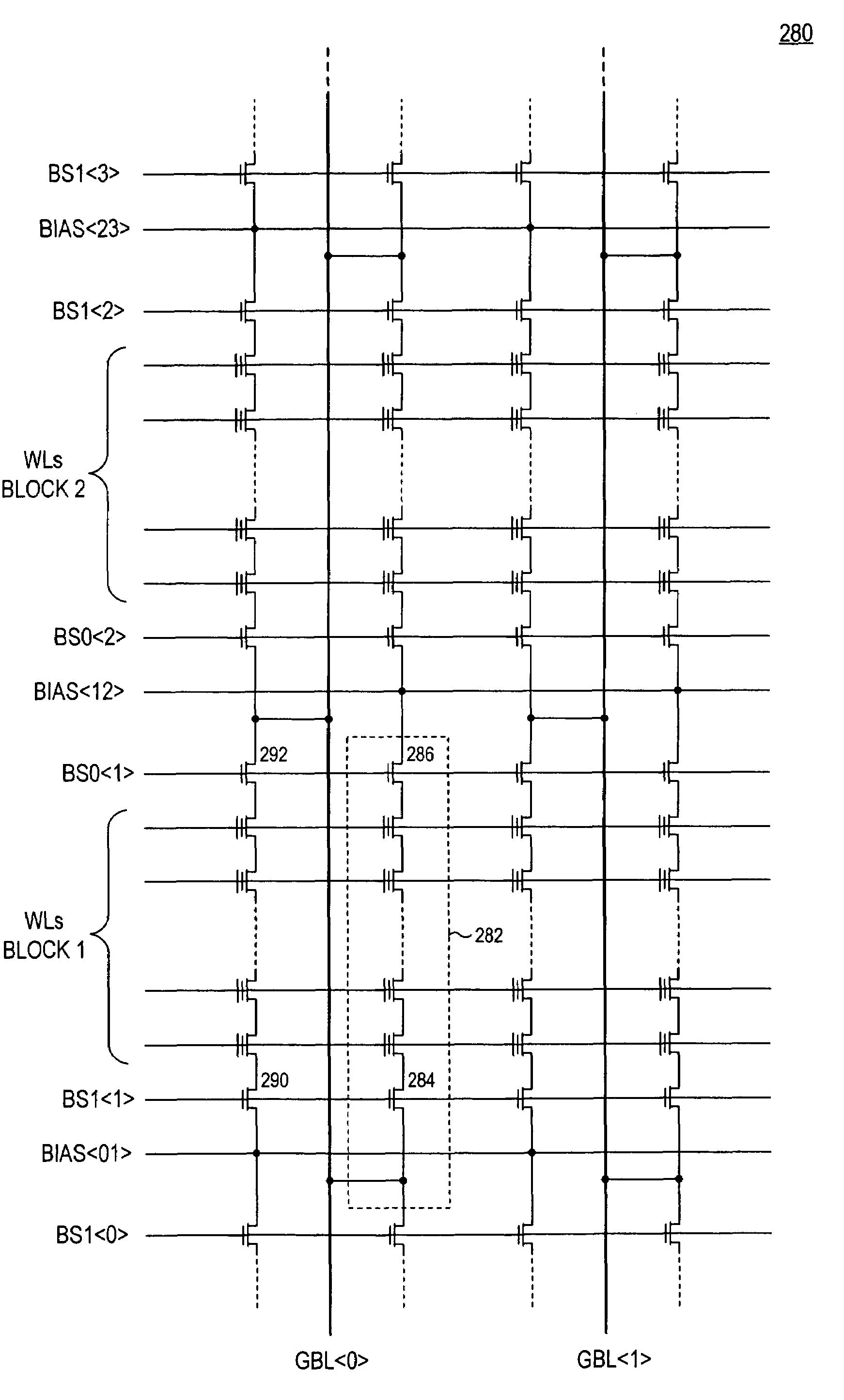
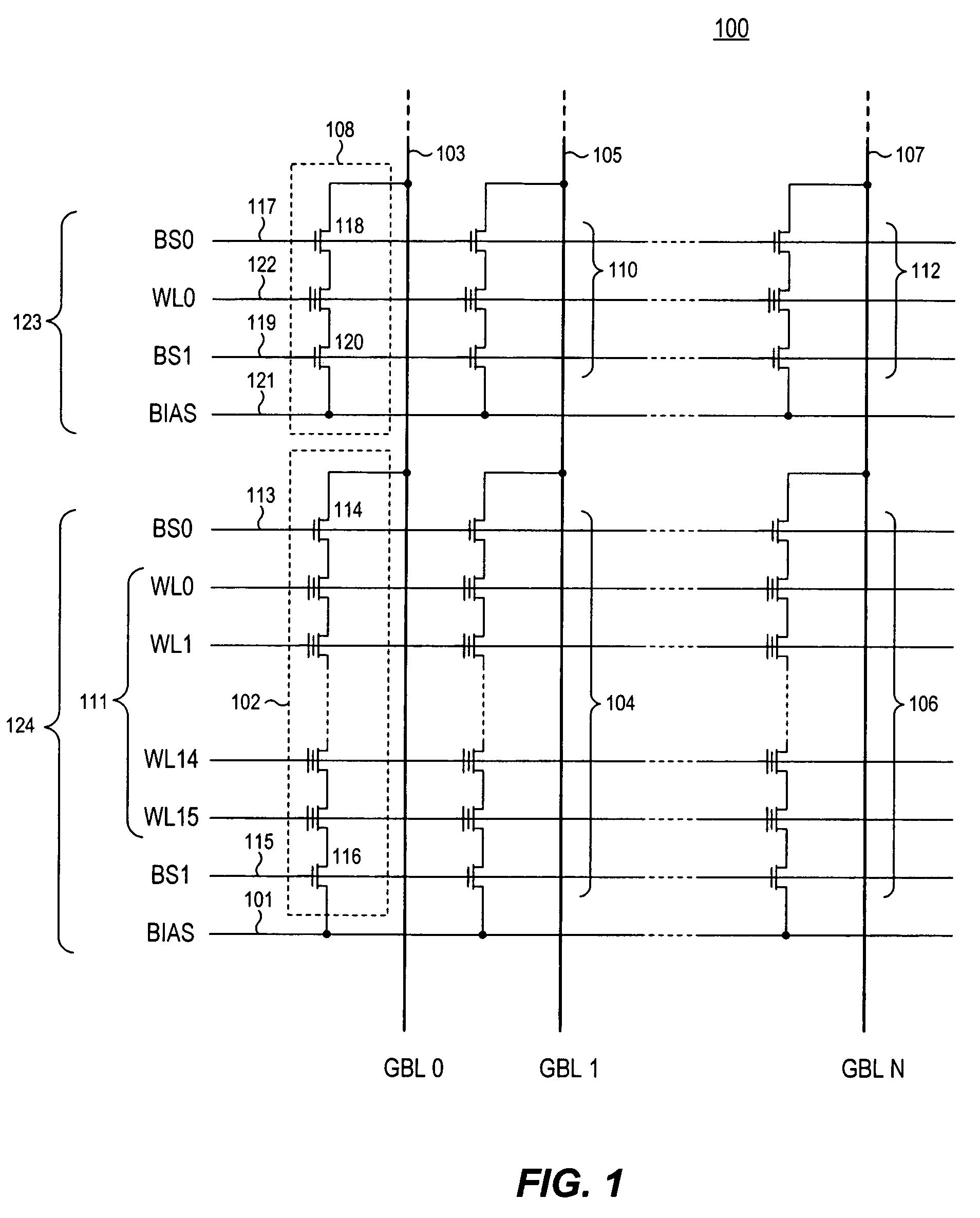
[0035]Referring now to FIG. 1, a schematic diagram is shown representing a portion of an exemplary memory array 100. The portion shown may represent a two-dimensional array having only one plane of memory cells, or may represent one level of three-dimensional memory array having more than one level (i.e., more than one plane) of memory cells. Series-connected NAND strings 102, 104, 106 each includes sixteen memory cell transistors connected in series, each gated by a respective one of a plurality of sixteen word lines 111 (individually labeled WL0, WL1, . . . , WL14, WL15). The NAND string 102 also includes a block select device 114 for coupling one end of the NAND string to a global bit line 103 (also labeled GBL0) in accordance with a block select signal BS0 conveyed on node 113, and further includes a second block select device 116 for coupling the other end of the NAND string to a shared bias node 101 in accordance with a block select signal BS1 conveyed on node 115.

[0036]Each ...


PUM


Abstract

A monolithic integrated circuit includes a memory array having first and second groups of NAND strings, each NAND string comprising at least two series-connected devices and coupled at one end to an associated global array line. NAND strings of the first and second groups differ in at least one physical characteristic, such as the number of series-connected devices forming the NAND string, but both groups are disposed in a region of the memory array traversed by a plurality of global array lines. The memory array may include a three-dimensional memory array having more than one memory plane. Some of the NAND strings of the first group may be disposed on one memory plane, and some of the NAND strings of the second group may be disposed on another memory plane. In some cases, NAND strings of both groups may share global array lines.

Description

BACKGROUND[0001]1. Field of the Invention[0002]The present invention relates to semiconductor integrated circuits containing memory arrays, and in preferred embodiments the invention particularly relates to monolithic three-dimensional memory arrays having series-connected strings of memory cells.[0003]2. Description of the Related Art[0004]Recent developments in semiconductor processing technologies and memory cell technologies have continued to increase the density achieved in integrated circuit memory arrays. For example, certain passive element memory cell arrays may be fabricated having word lines approaching the minimum feature size (F) and minimum feature spacing for the particular word line interconnect layer, and also having bit lines approaching the minimum feature width and minimum feature spacing for the particular bit line interconnect layer. Moreover, three-dimensional memory arrays having more than one plane or level of memory cells have been fabricated implementing s...

Claims


Application Information

Patent Timeline
Patent Type & Authority Patents(United States)
IPC IPC(8): G11C11/34
CPCH01L27/11551H01L27/11524G11C16/0483G11C11/005H10B41/35H10B41/20
Inventor FASOLI, LUCA G.SCHEUERLEIN, ROY E.
Owner SANDISK TECH LLC
Why Eureka
Try Eureka