

Erroneous operation preventing circuit of non-volatile memory device
- Summary
- Abstract
- Description
- Claims
- Application Information
AI Technical Summary
Benefits of technology
Problems solved by technology
Method used
Image

Examples
first embodiment
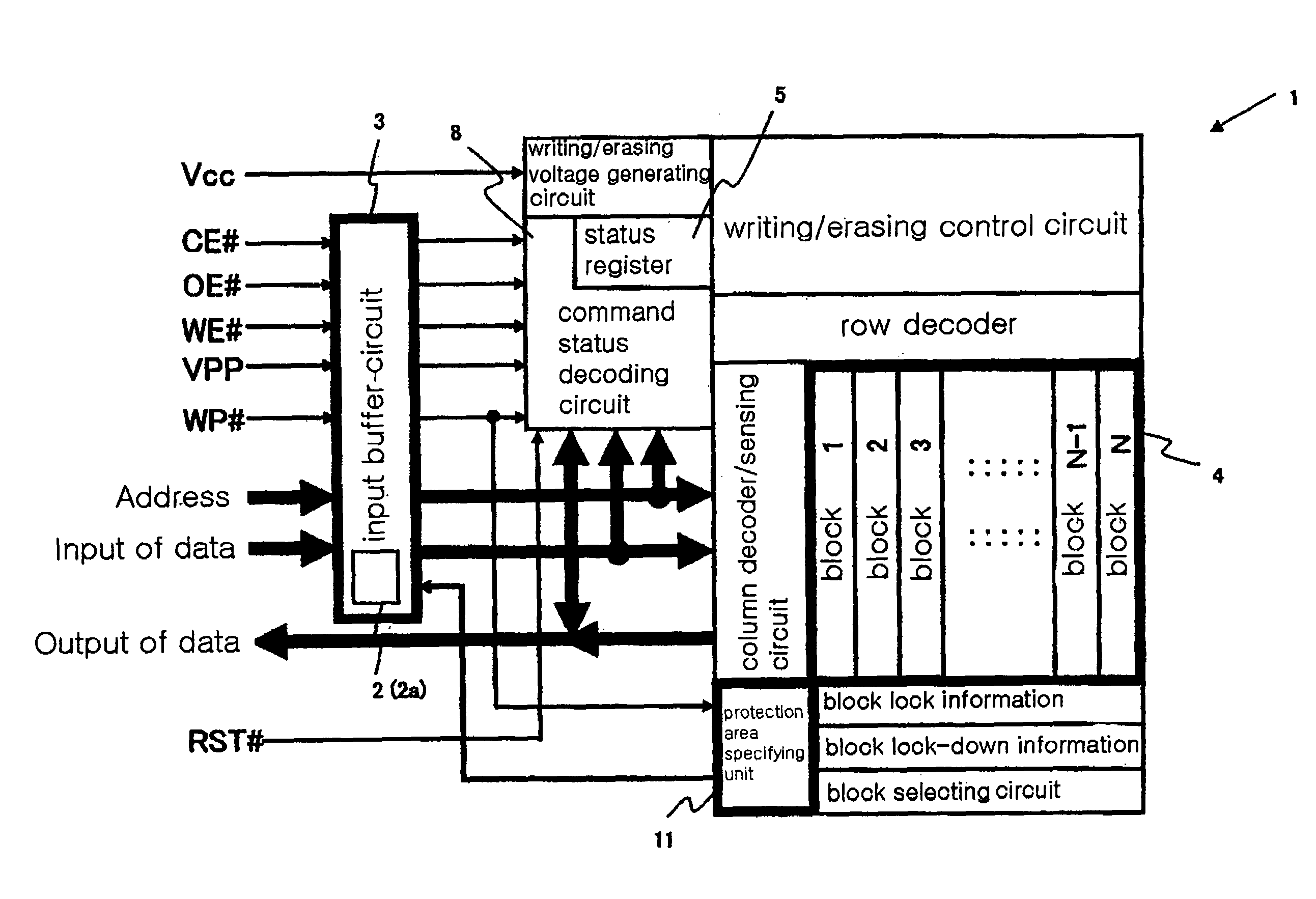
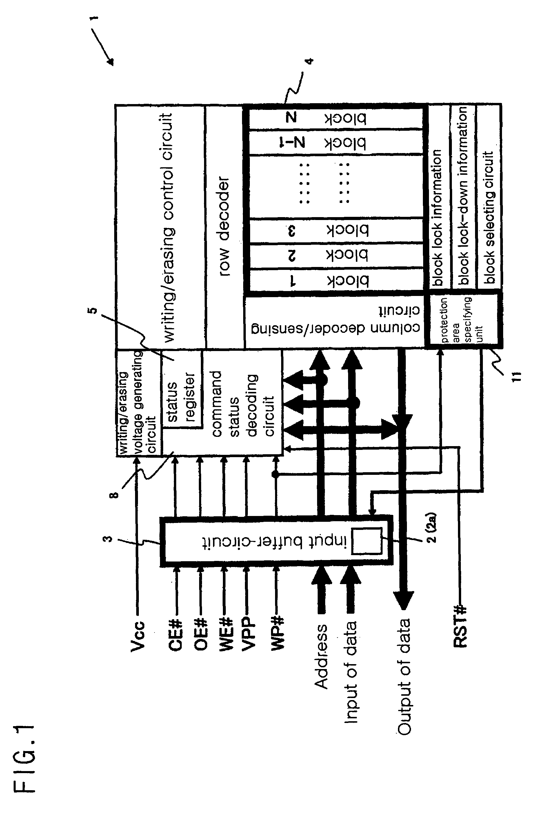
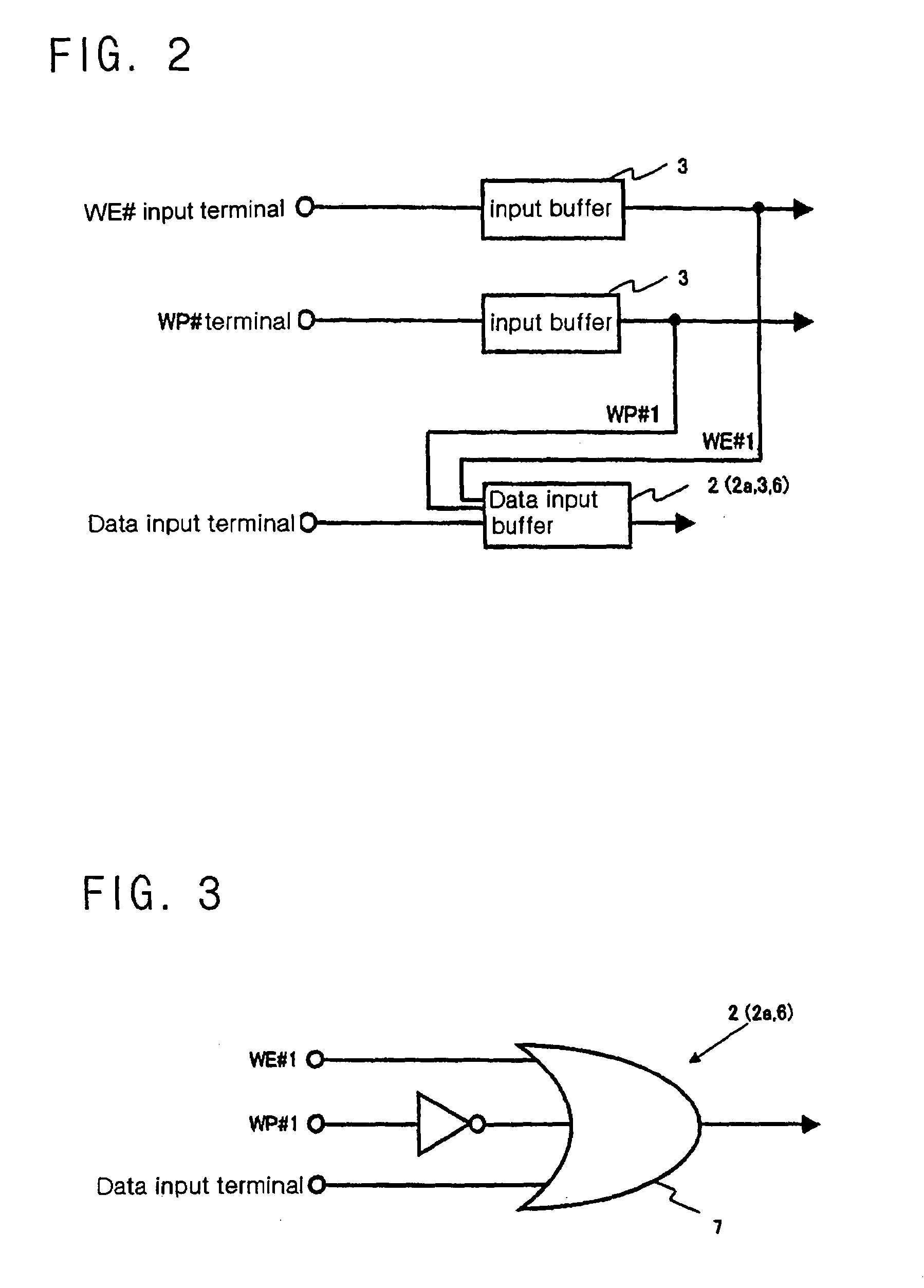
[0050]Now, the circuit 2 of the present invention will be described with reference to FIGS. 2 and 3. FIG. 2 is a block diagram illustrating a circuit configuration of the circuit 2 of the present invention, where the circuit 2 of the present invention comprises a data input buffer circuit 6 of an input buffer circuit 3, and is associated with an input buffer circuit having a WE# input terminal and an input buffer circuit having a WP# input terminal. Here, the data input buffer circuit 6 (an example of an operational mode enforcing circuit 2a) is generally controlled by means of a WP# input signal (which is an example of a control signal for protecting data and is a control signal specified for protecting data independently provided) from the WP# input terminal (a write protecting terminal) in addition to a WE# input signal from the WE# input terminal (which becomes active at a low level “0” and receives data (writing data or control commands) input from the data input terminal), so ...
second embodiment
[0053]Now, the circuit 2 of the present invention will be described with reference to FIGS. 4 and 5. FIG. 4 is a block diagram illustrating a circuit configuration of the circuit 2 of the present invention, where the circuit 2 of the present invention comprises a data input buffer circuit 6 of the input buffer circuit 3 and an input buffer circuit 9 having a WE# input terminal, and is associated with an input buffer circuit having the WP# input terminal and an input buffer circuit having the CE# input terminal. The data input buffer circuit 6 and the input buffer circuit 9 having the WE# input terminal constitute the operational mode enforcing circuit 2a. FIG. 5 is a logic circuit diagram illustrating a circuit configuration of the input buffer circuit 9 having the WE# input terminal. Here, the data input buffer circuit 6 has the same circuit configuration as shown in FIG. 3, similarly to the first embodiment.
[0054]When the WP# input signal turns into a low level “0”, as shown in FI...
third embodiment
[0056]Now, the circuit 2 of the present invention will be described with reference to FIGS. 6 and 7. FIG. 6 is a block diagram illustrating a circuit configuration of the circuit 2 of the present invention, where the circuit 2 of the present invention comprises a data input buffer circuit 6 (an example of the operational mode enforcing circuit 2a) in the input buffer circuit 3, and is associated with an input buffer circuit having a WE# input terminal and an input buffer circuit 10 having a VPP input terminal. FIG. 7 is a logic circuit diagram illustrating a circuit configuration of the data input buffer circuit 6. The third embodiment is different from the first embodiment, in that the VPP input signal from a VPP terminal for supply a writing / erasing high voltage is used in place of the WP# input signal from the WP# terminal. In addition, the flash memory 1 according to this embodiment is constructed such that when the VPP input signal is at a low level, a data protection status in...
PUM
 Abstract
Description
Claims
Application Information