Electro-optic displays, and components for use therein

a technology applied in the field of optical displays and components, can solve the problems of preventing their widespread use, insufficient service life of optical displays, and significant cos

Inactive Publication Date: 2007-03-13
E INK CORPORATION
View PDF180 Cites 276 Cited by
  • Summary
  • Abstract
  • Description
  • Claims
  • Application Information

AI Technical Summary

Benefits of technology

[0051]a gate electrode disposed on the opposed side of the gate dielectric layer from the channel region, such that variation of the voltage applied to the gate electrode can vary the conductivity of the channel region of the semiconductor layer, thus switching the transistor,

Problems solved by technology

Nevertheless, problems with the long-term image quality of these displays have prevented their widespread usage.
For example, particles that make up electrophoretic displays tend to settle, resulting in inadequate service-life for these displays.
Fabrication processes, however, can result in significant cost.
However, manufacturing flexible microelectronic backplanes for such displays presents many challenges.
A key problem in the manufacture and operation of such thin film transistors on flexible substrates is thin film cracking.

Method used


Image

  • Electro-optic displays, and components for use therein
  • Electro-optic displays, and components for use therein
  • Electro-optic displays, and components for use therein

Examples


Embodiment Construction

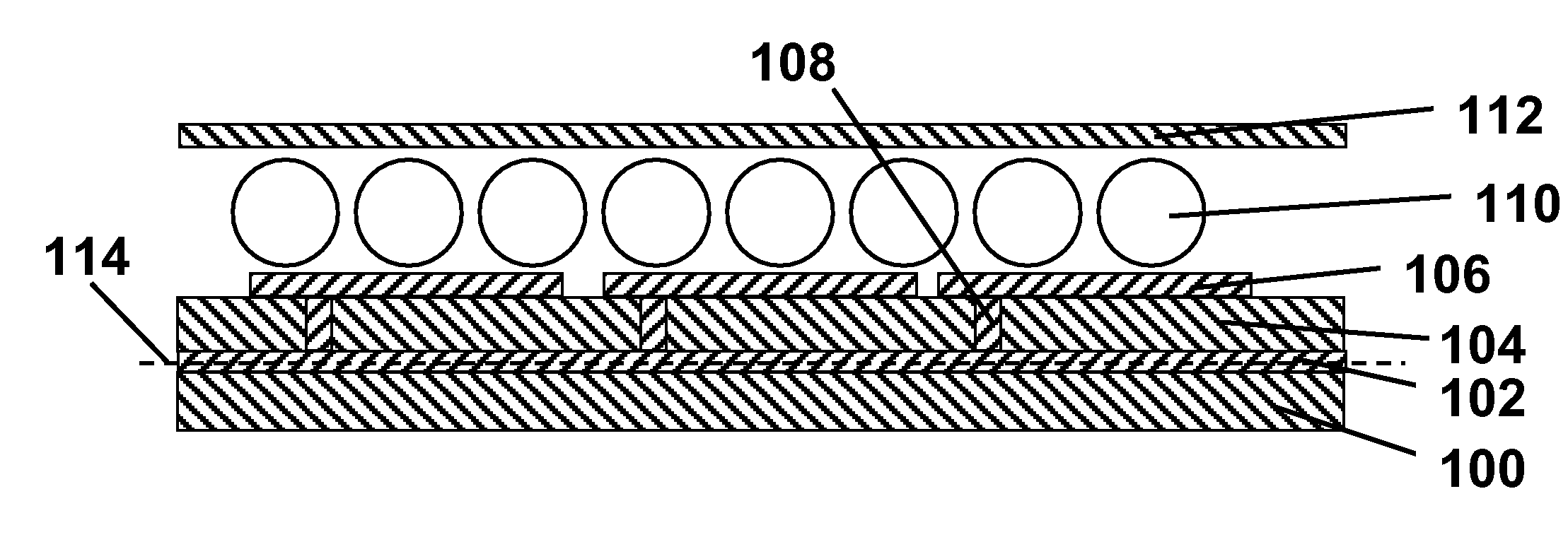
[0084]As already indicated, this invention has several different aspects electro-optic displays and to processes and components for the production of such displays. These various aspects will mainly be described separately below, but it should be understood that a single display, process or component may make use of more than one aspect of the invention. For example, FIG. 9 illustrates a single backplane which makes use of both the ring diode backplane and the narrow column electrode backplane aspects of the invention. To take another example, a controlled moduli display of the invention may be manufactured by an internal mask process of the invention.

[0085]Controlled Modulus Display

[0086]As already mentioned, this invention provides a controlled modulus electro-optic display comprising a substrate; a plurality of non-linear devices disposed substantially in one plane on the substrate; a plurality of pixel electrodes in electrical communication with the non-linear devices; a layer o...


PUM

PropertyMeasurementUnit
thicknessaaaaaaaaaa
thicknessaaaaaaaaaa
widthaaaaaaaaaa

Abstract

An electro-optic display comprises a substrate (100), non-linear devices (102) disposed substantially in one plane on the substrate (100), pixel electrodes (106) connected to the non-linear devices (102), an electro-optic medium (110) and a common electrode (112) on the opposed side of the electro-optic medium (110) from the pixel electrodes (106). The moduli of the various parts of the display are arranged so that, when the display is curved, the neutral axis or neutral plane lies substantially in the plane of the non-linear devices (102).

Description

REFERENCE TO RELATED APPLICATIONS[0001]This application is a continuation-in-part of copending application Ser. No. 10 / 249,618, filed Apr. 24, 2003 (Publication No. 2003 / 0222315), which claims benefit of Application Ser. Nos. 60 / 375,571 and 60 / 375,508, both filed May 12, 2002.[0002]This application also claims benefit of Application Ser. No. 60 / 481,565, filed Oct. 27, 2003 and Application Ser. No. 60 / 481,591, filed Nov. 3, 2003.[0003]This application is also related to (a) copending application Ser. No. 10 / 249,624 filed Apr. 24, 2003 (Publication No. 2004 / 0014265), which claims benefit of Application Ser. No. 60 / 375,248, filed Apr. 24, 2002, and Application Ser. No. 60 / 376,603, filed Apr. 30, 2002; (b) copending application Ser. No. 09 / 565,413, filed May 5, 2000 (cf. published International Application WO 00 / 67327; (c) application Ser. No. 09 / 904,109, filed Jul. 12, 2001 (now U.S. Pat. No. 6,683,333); (d) copending application Ser. No. 10 / 065,795, filed Nov. 20, 2002 (Publication No...

Claims


Application Information

Patent Timeline
Patent Type & Authority Patents(United States)
IPC IPC(8): H01L27/148H01L29/768G02F1/167H01L21/77H01L21/84H01L27/12H01L29/417H01L29/423
CPCH01L27/12H01L29/41733H01L29/42384H01L27/1292H01L33/48H01L21/02104H01L27/1285H01L29/78603G02F1/167G02F1/1681H01L27/1214G02F1/1368H01L21/30604H01L21/308H01L27/124H01L27/1259H01L27/1222H01L27/127H01L29/78666
Inventor AMUNDSON, KARL R.RITENOUR, ANDREW P.DUTHALER, GREGG M.DRZAIC, PAUL S.CHEN, YUKAZLAS, PETER T.
Owner E INK CORPORATION
Why Eureka
Try Eureka