Single-poly EEPROM cell with lightly doped MOS capacitors

a single-poly eeprom and capacitor technology, applied in the field of memory cells, can solve the problems of not being completely realized, control capacitor oxide cannot be easily stored on the single poly layer, and single-poly eeprom may not be completely manufactured with a standard cmos process flow, etc., to achieve the effect of reducing the need for large bias voltage, reducing damage, and altering the conduction properties of mosfet transistors

Active Publication Date: 2007-03-01
HONEYWELL INT INC
View PDF12 Cites 7 Cited by
  • Summary
  • Abstract
  • Description
  • Claims
  • Application Information

AI Technical Summary

Benefits of technology

[0010] Various arrangements of capacitors are disclosed in this application. The EEPROM memory cell can be manufactured with one or more tunneling capacitors as well as one or more control capacitors. Multiple tunneling capacitors allow for selective tunneling paths. Additionally, multiple control capacitors operated in parallel allow for reduced variation in capacitance when biased in or around inversion.
[0012] A method for applying bias to the bottom plates of the capacitors within an EEPROM memory cell is also disclosed. This method may reduce the need for large bias voltages and it also prevents electrons from tunneling through the oxide of the FET gate capacitor. In addition, this method reduces damage that may occur at the gate oxide of the MOSFET. This damage may alter the conduction properties of the MOSFET transistor.

Problems solved by technology

Thus far, however, this goal may not be completely realized.
However, this particular single-poly EEPROM may not be completely manufacturable with a standard CMOS process flow in that it requires additional fabrication steps to support the oxide on top of the n+ diffusion 214 that forms part of the control capacitor 208.
That is, the control capacitor oxide does not easily allow charge stored on the single poly layer 212 to leak away.
This damage may alter the conduction properties of the MOSFET transistor.

Method used


Image

  • Single-poly EEPROM cell with lightly doped MOS capacitors
  • Single-poly EEPROM cell with lightly doped MOS capacitors
  • Single-poly EEPROM cell with lightly doped MOS capacitors

Examples


Embodiment Construction

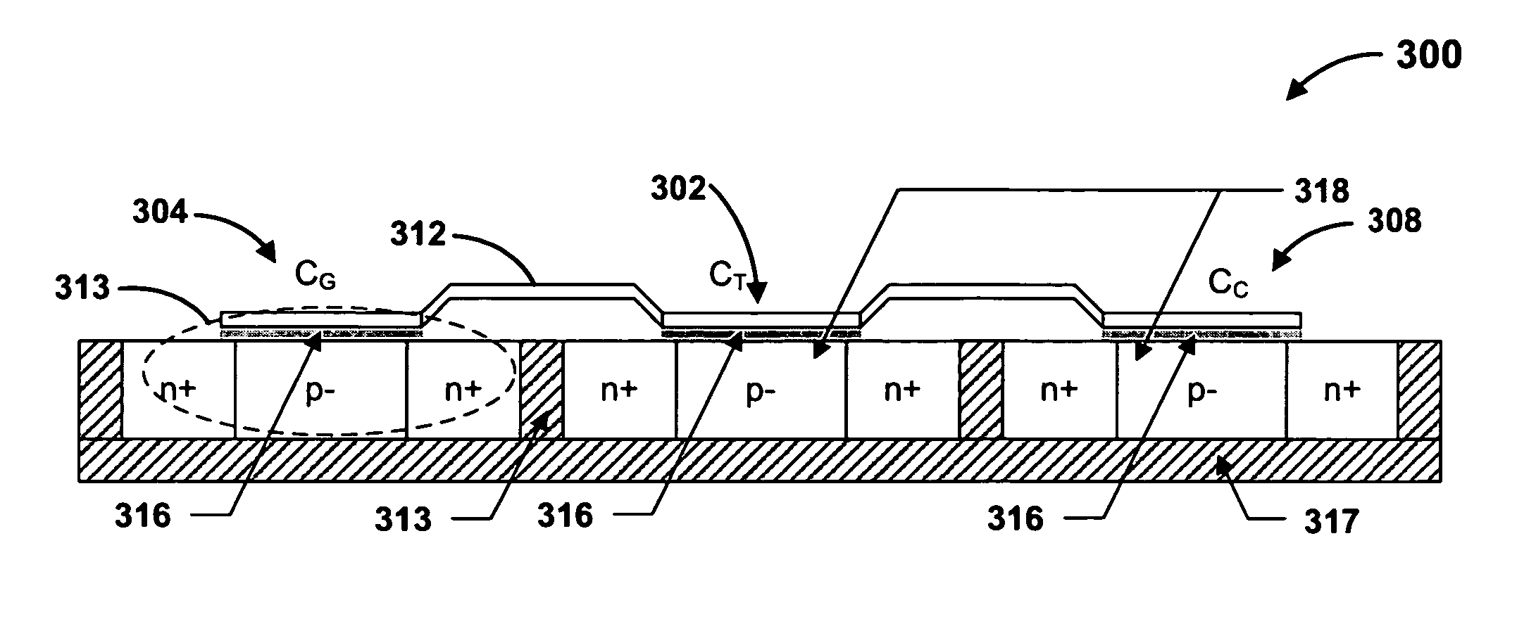
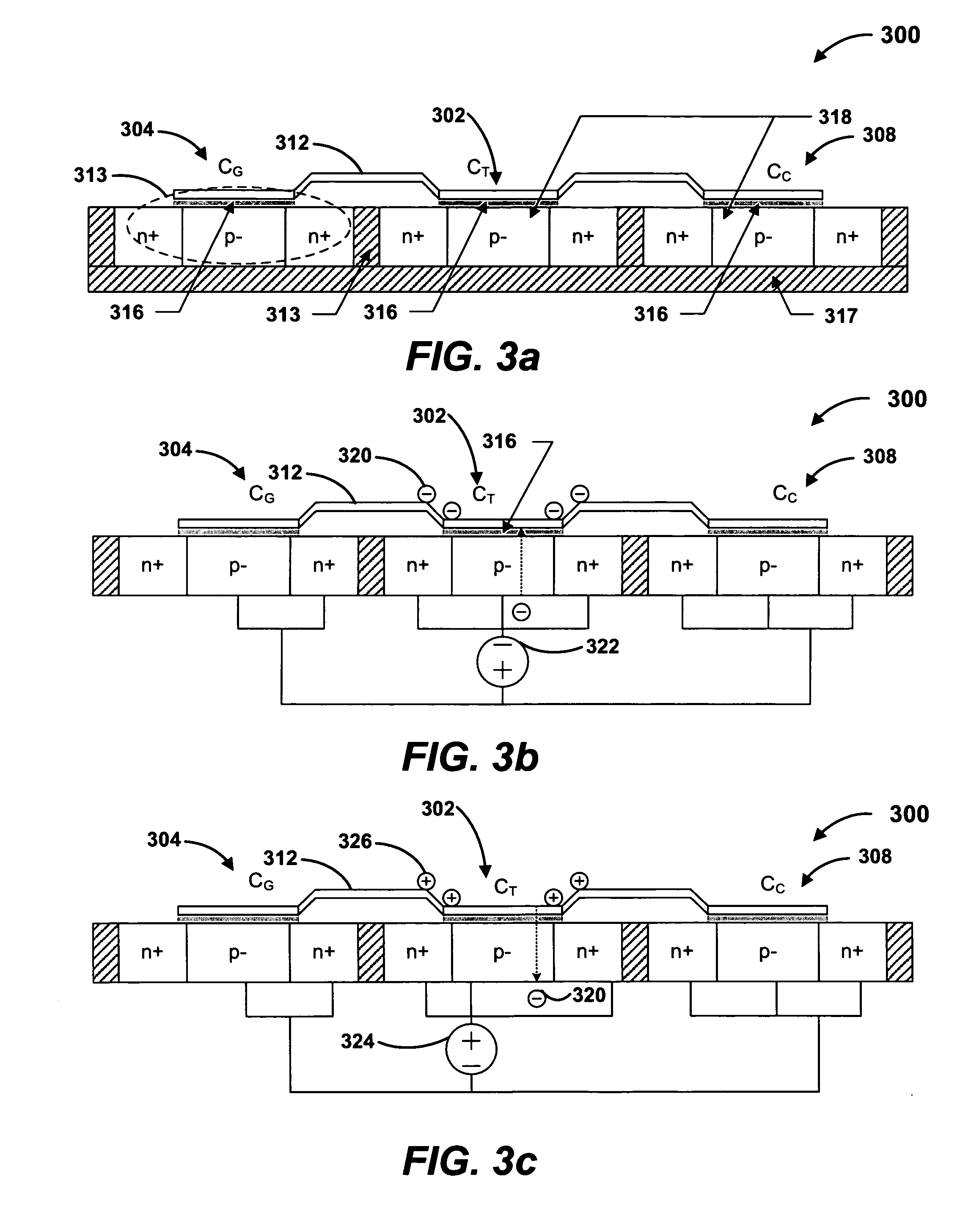
[0039] An EEPROM memory cell that is manufacturable in a standard CMOS process is presented. MOS capacitors are connected to each other via a single polysilicon line. Each capacitor has an oxide layer that is typically the thickness of the gate oxide of a FET transistor. Beneath the oxide layer is a lightly doped region. The lightly doped region may be manufactured in a standard process, such as a standard well implant, or it may even be the background doping of a semiconductor substrate. All of these processing methods, particularly when combined, allow an EEPROM cell to be created in a standard CMOS process.

[0040] One advantage of creating an EEPROM cell in a standard CMOS process is that a circuit designer can use the same semiconductor processing steps for a particular Application Specific Integrated Circuit (ASIC) and an array of EEPROM memory cells. This would allow both devices to be created side by side without altering a process flow. Altering the process flow includes add...


PUM


Abstract

An Electrically Erasable Programmable Read Only Memory (EEPROM) memory cell and a method of operation are disclosed for creating an EEPROM memory cell in a standard CMOS process. A single polysilicon layer is used in combination with lightly doped MOS capacitors. The lightly doped capacitors employed in the EEPROM memory cell can be asymmetrical in design. Asymmetrical capacitors reduce area. Further capacitance variation caused by inversion can also be reduced by using multiple control capacitors. In addition, the use of multiple tunneling capacitors provides the benefit of customized tunneling paths.

Description

GOVERNMENT RIGHTS [0001] The United States Government has acquired certain rights in this invention pursuant to Contract No. DE-FC26-03NT41834 and DE-FC26-03NT41835 awarded by the Department of Energy.BACKGROUND [0002] 1. Field of Invention [0003] The present invention relates to the field of memory cells, and specifically to a single-poly memory cell fabricated in a standard CMOS process flow. [0004] 2. Description of Related Art [0005] One of the recent developments in Electrically Erasable Programmable Read Only Memory (EEPROM) cells has been the use of a single polysilicon deposition process to form a link between a control capacitor, a tunneling capacitor and an EEPROM Field Effect Transistor (FET). Because there may be no direct electrical connections to the single-poly layer, it is referred to as a ‘floating gate’. The floating gate also forms the gate of the EEPROM FET. Before the use of a single poly layer, an EEPROM cell was typically constructed from two poly layers. One ...

Claims


Application Information

Patent Timeline
Patent Type & Authority Applications(United States)
IPC IPC(8): H01L29/788
CPCH01L27/115H01L27/11521H01L29/7883H01L27/1203H01L27/11558H10B41/60H10B69/00H10B41/30
Inventor RIEKELS, JAMES E.LUCKING, THOMAS B.LARSEN, BRADLEY J.GARDNER, GARY R.
Owner HONEYWELL INT INC
Why Eureka
Try Eureka