Method for improving luminance of AlGaInP quaternary single-face dual-electrode light-emitting diode with GaAs substrate

A technology of light-emitting diodes and double electrodes, applied in circuits, electrical components, electrical solid devices, etc., can solve the problems of DBR layer conductivity and reflectivity, elimination of Joule heat without improvement, and reduction of AlGaAs refractive index.

Active Publication Date: 2014-01-01
SHANDONG INSPUR HUAGUANG OPTOELECTRONICS
View PDF6 Cites 7 Cited by
  • Summary
  • Abstract
  • Description
  • Claims
  • Application Information

AI Technical Summary

Problems solved by technology

Chinese patent CN1355569 discloses a high-reflection Bragg reflector structure, which is characterized in that a part of the Bragg reflector is oxidized to increase the reflectivity, but this method does not play a very obvious role, and the AlGaAs refractive index after oxidation decreases , and losses in this layer (losses including scattering and absorption) and Joule heating from series resistance do not reduce much
This patent only provides an improved Al 2 o 3 / GaAs DBR layer interface quality method, that is, the AlAs / GaAs DBR layer is directly annealed in the oxidation furnace after wet oxidation. This method only eliminates the stress at the DBR interface, but does not affect the conductivity and reflection of the DBR layer. rate, Joule heat elimination, etc. have no improvement effect

Method used


Image

  • Method for improving luminance of AlGaInP quaternary single-face dual-electrode light-emitting diode with GaAs substrate
  • Method for improving luminance of AlGaInP quaternary single-face dual-electrode light-emitting diode with GaAs substrate
  • Method for improving luminance of AlGaInP quaternary single-face dual-electrode light-emitting diode with GaAs substrate

Examples


Embodiment Construction

[0012] Technical scheme of the present invention is as follows:

[0013] A method for improving the brightness of a GaAs substrate AlGaInP quadruple single-sided double-electrode light-emitting diode, comprising the following steps:

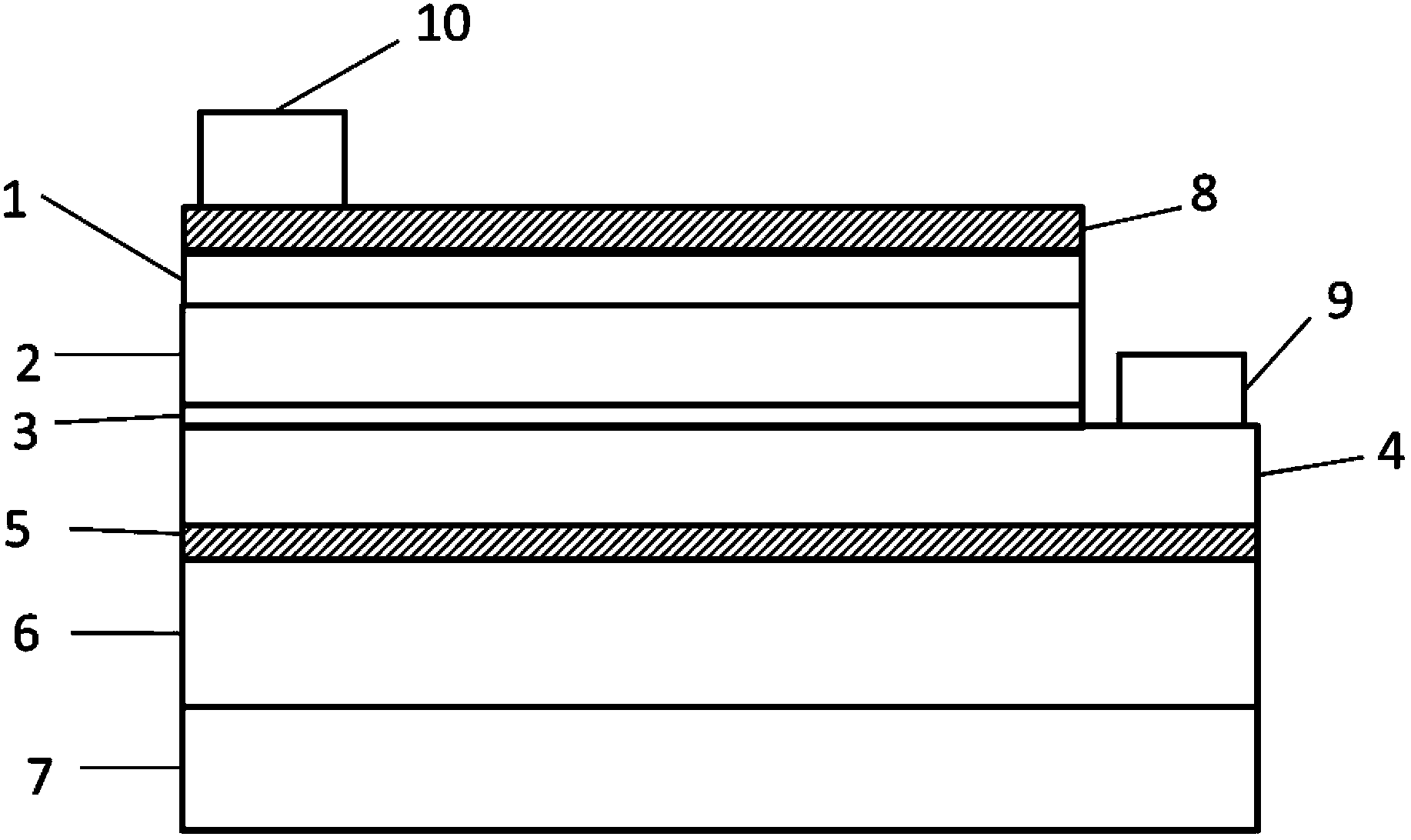
[0014] (1) The GaAs layer, DBR layer, N-type AlGaIn layer, quantum well active region, P-type AlGaIn layer and GaP layer are sequentially prepared on the GaAs substrate by MOCVD method, and the P electrode is made on the GaP layer, and the N-type A mesa is formed on the AlGaIn layer, and an N electrode is formed on the mesa to make a light emitting diode;

[0015] (2) half-cutting the light-emitting diodes in step (1) along the upper surface of the DBR layer, the depth of half-cutting is in the range of 20-40 μm; half-cutting the light-emitting diodes along the upper surface of the DBR layer, realizing the The horizontal circumcision of the light-emitting diode makes the upper surface of the DBR layer and the N-type AlGaIn layer form a gap to pr...


PUM


Abstract

The invention relates to a method for improving the luminance of an AlGaInP quaternary single-face dual-electrode light-emitting diode with a GaAs substrate. The oxidized DBR layer technology, the electrode structuralization technology, the high current expansion technology, the same-face dual-electrode technology and the like are integrated, LED open circuits or LED half open circuits are avoided, and the dual-electrode light-emitting diode can become a high-luminance same-face dual-electrode light-emitting diode which is high in reflection and free from Joule heat. After the steps of epitaxial growth and electrode manufacture of a high-luminance light-emitting diode chip are completed, the chip undergoes half cutting and finally undergoes one time of oxidization, the conductivity of the DBR layer is changed so that the DBR layer becomes an insulating layer, the reflection ratio is greatly improved, loss caused by generation of the Joule heat, scattering and the like is eliminated, and 100% luminous efficiency is achieved.

Description

technical field [0001] The invention relates to a method for improving the brightness of a GaAs substrate AlGaInP quadruple single-sided double-electrode light-emitting diode, which belongs to the technical field of optoelectronic devices. Background technique [0002] Due to its advantages of high efficiency, energy saving, and environmental protection, light-emitting diodes have been widely used in automobile and traffic signal indication, large-screen display, backlighting of liquid crystal display, solid-state lighting and other fields. Quaternary alloy materials (Al x Ga 1-x ) 0.5 In 0.5 P has a wide direct bandgap, covers the visible light wavelength range of 560-650nm, and can completely match the lattice of GaAs substrate. It is an excellent material for preparing red to green band LEDs. The light extraction efficiency of AlGaInP LED is very low due to the difference between the refractive index of semiconductor and air, which makes the light exit cone of the lig...

Claims


Application Information

Patent Timeline
Patent Type & Authority Applications(China)
IPC IPC(8): H01L33/10H01L33/38H01L33/62
CPCH01L33/0062H01L33/10H01L33/38H01L33/62H01L2224/48091H01L2224/48247H01L2924/00014
Inventor 闫宝华夏伟徐现刚李懿洲汤福国
Owner SHANDONG INSPUR HUAGUANG OPTOELECTRONICS
Why Eureka
Try Eureka