Magnetoresistive effect element, magnetic head and magnetic reproducing apparatus

a technology of magnetic head and reproducing apparatus, applied in the field of magnetoresistive effect element, magnetic head and magnetic recording apparatus, can solve the problems of difficult to obtain a large reproduction output signal, difficult to form uniform pinholes, and noise of shots

Inactive Publication Date: 2007-03-13
KK TOSHIBA
View PDF21 Cites 31 Cited by
  • Summary
  • Abstract
  • Description
  • Claims
  • Application Information

AI Technical Summary

Benefits of technology

[0013]According to another embodiment of the invention, there is provided a magnetoresistive effect element comprising: a magnetoresistive effect film including a magnetization-pinned layer having a magnetic film pinned in magnetization substantially in one direction, a magnetization free layer having a magnetic film variable in direction of magnetization in response to an external magnetic field, and a nonmagnetic metal intermediate layer interposed between said magnetization-pinned layer and said magnetization free layer; and a pair of electrodes electrically coupled to said magnetoresistive effect film to supply a current substantially perpendicularly to the film plane of said magnetoresistive effect film, a first layer which contains a half-metal as a major component thereof being interposed in at least one of a location between said magnetization-pinned layer and said nonmagnetic metal intermediate layer and a location between said magnetization free layer and said nonmagnetic metal intermediate layer.

Problems solved by technology

However, in case of TMR elements, the insulator used as the intermediate layer excessively increase the device resistance, and it is its difficulty that downsizing of the device area causes shot noise peculiar to the tunneling phenomenon due to a large resistance, or deterioration of the response to high frequencies.
As a result, it is difficult to obtain a large reproduction output signal.
However, it is difficult to form uniform pinholes.
Thus, it is a hurdle against its practical use that the resistance largely varies when the recording density increases to or beyond 100 Gbpsi, where the device size is in the order of 0.1 μm, and uniform CPP elements are difficult to manufacture.

Method used


Image

  • Magnetoresistive effect element, magnetic head and magnetic reproducing apparatus
  • Magnetoresistive effect element, magnetic head and magnetic reproducing apparatus
  • Magnetoresistive effect element, magnetic head and magnetic reproducing apparatus

Examples


first embodiment

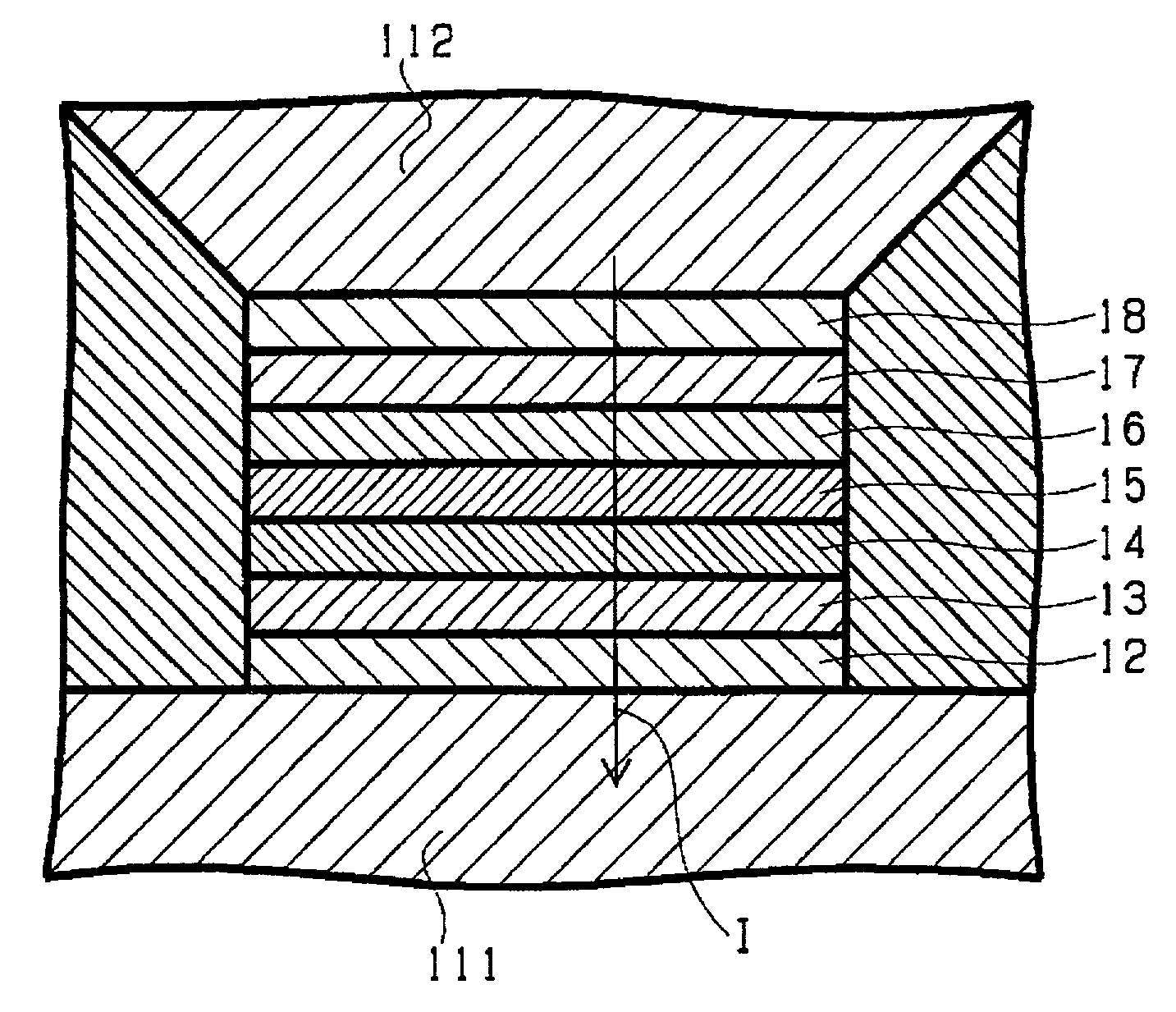
[0030]FIG. 1A is a schematic diagram that shows a cross-sectional structure of the substantial part of a magnetoresistive effect element according to the invention. FIG. 1A is a cross-sectional view taken along a plane parallel to the medium-facing surface of the magnetoresistive effect element assumed to be used in a magnetic head.

[0031]As illustrated here, the magnetoresistive effect element according to the embodiment of the invention includes a magnetoresistive effect film made by sequentially depositing on a lower electrode 111 a base layer 12, free layer 13 variable in magnetization in response to an external signal magnetic field, nonmagnetic intermediate layer 14, pinned layer 15 substantially fixed in magnetization against an external signal magnetic field, magnetic coupling intermediate layer 16, antiferromagnetic layer 17, and protective film 18. The protective film 18 is not indispensable if the antiferromagnetic layer 17 does not deteriorate in property upon deposition ...

second embodiment

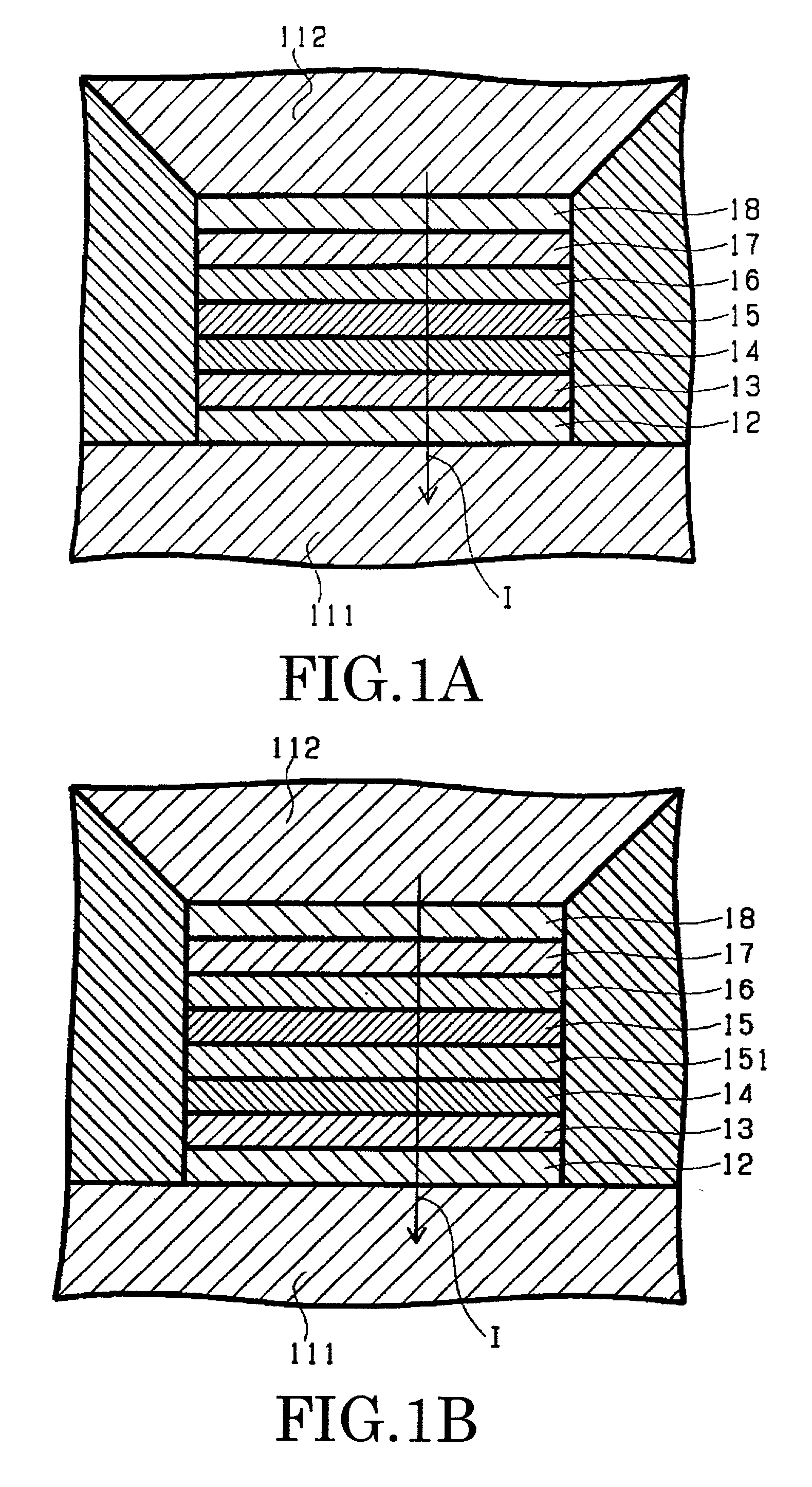
[0064]FIG. 2 is a schematic diagram that shows a cross-sectional structure of the substantial part of a magnetoresistive effect element according to the invention. This is also a cross-sectional view taken along a plane parallel to the medium-facing surface of the magnetoresistive effect element assumed to be used in a magnetic head. Some of components shown here, which are common to those of FIG. 1A, are labeled with common reference numerals, and their detailed explanation is omitted here.

[0065]The magnetoresistive effect element 10B according to this embodiment is opposite from the element of FIG. 1A in the stacking order of respective layers or films. More specifically, sequentially formed on the lower electrode 111 are the base layer 12, antiferromagnetic layer 17, magnetic coupling intermediate layer 16, pinned layer 15, nonmagnetic intermediate layer 14, free layer 13, and protective layer 18. Then the upper electrode 112 is formed thereon. Even when the stacking order is rev...

third embodiment

[0067]Next explained is a magnetoresistive effect element according to the invention.

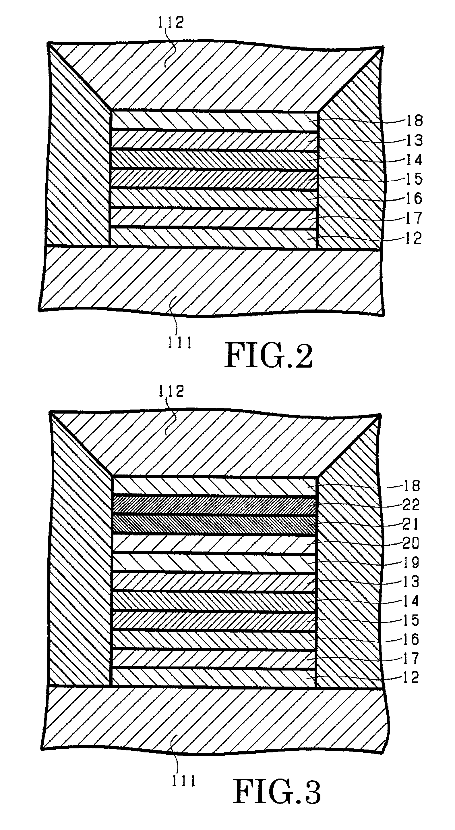
[0068]FIG. 3 is a schematic diagram that shows a cross-sectional structure of the substantial part of the magnetoresistive effect element according to the third embodiment of the invention. Here again, some of components shown here, which are common to those of FIG. 1A to FIG. 2, are labeled with common reference numerals, and their detailed explanation is omitted here.

[0069]The magnetoresistive effect element 10C according to this embodiment has a structure made by additionally stacking, on the free layer 13 of the magnetoresistive effect element 10B of FIG. 2, a second nonmagnetic metal intermediate layer 19, second pinned layer 20 made of a half-metal similar to that of the pinned layer 15, second magnetic coupling intermediate layer 21 similar to the magnetic coupling intermediate layer 16, second antiferromagnetic layer 21 similar to the antiferromagnetic layer 17, and protective film 18 in the...


PUM

PropertyMeasurementUnit
thicknessaaaaaaaaaa
thicknessaaaaaaaaaa
Thicknessaaaaaaaaaa

Abstract

In a CPP element using a metal intermediate layer excellent in shot noise and response to high frequencies unlike a TMR element, its magnetoresistive effect film includes a magnetic layer mainly made of a half-metal exhibiting ferromagnetism, ferrimagnetism or antiferromagnetism, and largely variable in way of conduction in response to spin direction of electrons.

Description

CROSS-REFERENCE TO RELATED APPLICATIONS[0001]This application is based upon and claims the benefit of priority from the prior Japanese Patent Application No. 2001-190512, filed on Jun. 22, 2001; the entire contents of which are incorporated herein by reference.BACKGROUND OF THE INVENTION[0002]This invention relates to a magnetoresistive effect element, magnetic head and magnetic recording apparatus, and more particularly, to a magnetoresistive effect element structured to flow a sense current vertically of the film surface of a magnetoresistive effect film, as well as a magnetic head and a magnetic reproducing apparatus using the magnetoresistive effect element.[0003]Following to the discovery of giant magnetoresistive effects (GMR) in multi-layered structures of magnetic layers, there is an epoch-making progress in performance of magnetic devices, especially of magnetic heads. Especially, discovery of GMR by spin-valve (SV) films brought about a large technical progress in the fiel...

Claims


Application Information

Patent Timeline
Patent Type & Authority Patents(United States)
IPC IPC(8): G11B5/33G01R33/09G11B5/012G11B5/39H01F10/20H01F10/32H01L43/08H01L43/10
CPCB82Y10/00B82Y25/00H01L43/10G11B5/3909H01F10/3254G11B5/3903G11B5/012G11B2005/3996H10N50/10H10N50/85
Inventor IWASAKI, HITOSHIKOUI, KATSUHIKOYOSHIKAWA, MASATOSHIYUASA, HIROMIFUKUZAWA, HIDEAKISAHASHI, MASASHI
Owner KK TOSHIBA
Why Eureka
Try Eureka