Thermal heat spreaders designed for lower cost manufacturability, lower mass and increased thermal performance

a heat spreader and heat dissipation device technology, applied in the direction of cooling/ventilation/heating modification, semiconductor/solid-state device details, semiconductor devices, etc., can solve the problems of increasing the density of the circuit in the device, reducing the reliability and performance of the device, and adding excess weight and cos

Inactive Publication Date: 2007-03-13
INTEL CORP
View PDF14 Cites 32 Cited by
  • Summary
  • Abstract
  • Description
  • Claims
  • Application Information

AI Technical Summary

Problems solved by technology

This results in an increased density of circuits in the device.
Unfortunately, device reliability and performance will decrease as the amount of heat that the device is exposed to increases.
First, the contiguous wall 106a associated with the heat spreader body 105a adds little to the dissipation of heat. Its main purpose is to act as a support for the heat spreader body 105a, and as a point of attachment to the substrate 101a. This adds excess weight and cost, as well as contributes to manufacturing defects through the addition of unneeded complexity in forming the contiguous wall structure. In addition, bonding a contiguous wall structure to a substrate results in a very rigid package, which can lead to package failure when thermally stressed due to differences in the coefficient of thermal expansion (CTE) between the heat spreader and substrate materials.
Second, the bond line thickness 104a between the integrated circuit 103a and the heat spreader 105a is strongly influenced by the size of the metal particles 206a that are a constituent of the thermal interface material used to form the bond between the integrated circuit 101a and the heat spreader 105a. This works well as long as the particle size 206a is relatively uniform. However, referring to FIG. 2b, when there is a wide distribution of metal particle 206b size, a condition called “die tilting” may occur. Die tilting is caused by a relatively large particle 206b in the thermal interface material becoming wedged in between the integrated circuit 101b and the heat spreader 105b. When a clamping pressure is applied to the heat spreader 105b during the manufacturing process, the large particle 206b causes an uneven distribution of force across the face of the integrated circuit 101b, either causing the device 103b to tilt to relieve the stress, or perhaps to crack. This die tilting or cracking may lead to either poor device reliability or to complete failure.

Method used


Image

  • Thermal heat spreaders designed for lower cost manufacturability, lower mass and increased thermal performance
  • Thermal heat spreaders designed for lower cost manufacturability, lower mass and increased thermal performance
  • Thermal heat spreaders designed for lower cost manufacturability, lower mass and increased thermal performance

Examples


Embodiment Construction

[0024]An improved apparatus for spreading heat from a packaged integrated circuit is described. In the following description, numerous specific details are set forth such as material types, dimensions, etc., in order to provide a thorough understanding of the present invention. However, it will be obvious to one of skill in the art that the invention may be practiced without these specific details. In other instances, well-known elements and processing techniques have not been shown in particular detail in order to avoid unnecessarily obscuring the present invention.

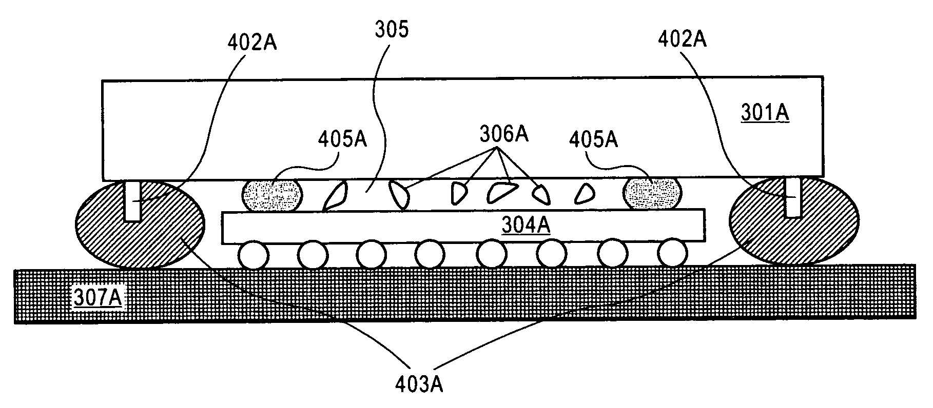
[0025]A heat spreader, comprising a metal body with attached standoffs located approximately above the integrated circuit, is described. The standoffs should improve bond layer thickness control between the integrated circuit and the heat spreader, leading to a lower cost and lower mass package, as well a more reliable device with increased thermal performance.

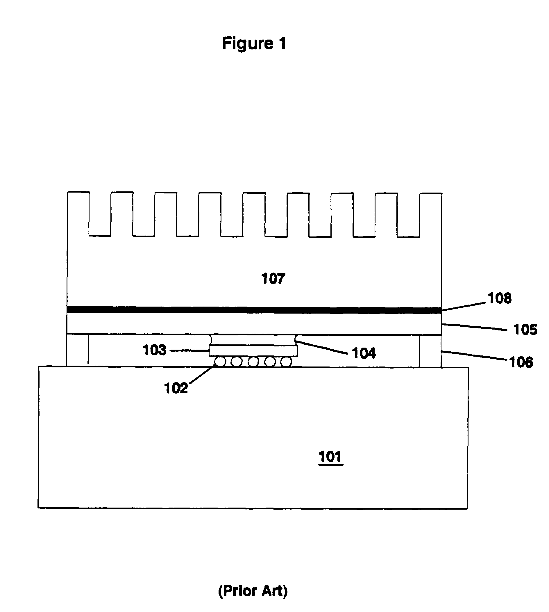
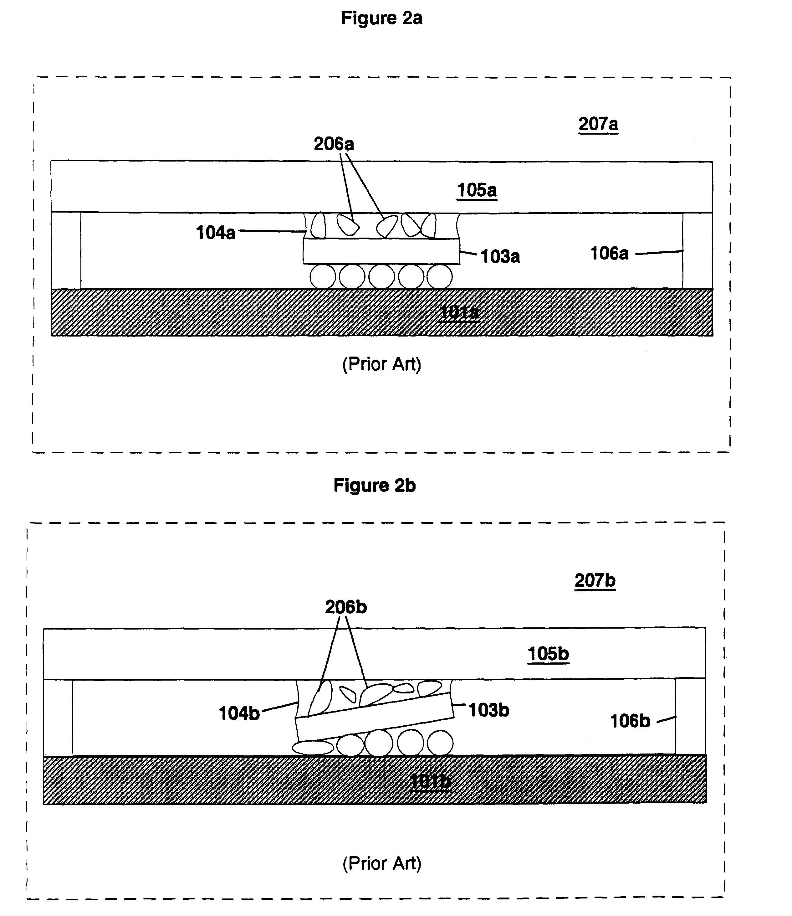
[0026]This discussion will mainly be limited to those needs a...


PUM


Abstract

A heat spreader, comprising a metal body with attached standoffs located approximately above the integrated circuit, is described. The standoffs should improve bond layer thickness control between the integrated circuit and the heat spreader, leading to a lower cost and lower mass package, as well as a more reliable device with increased thermal performance.

Description

CROSS-REFERENCE TO RELATED APPLICATIONS[0001]The present patent application is a divisional of prior application Ser. No. 09 / 675,316, filed Sep. 29, 2000, now abandonded entitled “THERMAL HEAT SPREADERS DESIGNED FOR LOWER COST MANUFACTURABILITY, LOWER MASS AND INCREASED THERMAL PERFORMANCE.”BACKGROUND[0002]1. Field of the Invention[0003]This invention relates to semiconductor manufacturing technology generally, and more specifically, to heat spreader technology for heat dissipation in a semiconductor package.[0004]2. Description of the Related Art[0005]There is a trend toward increasing the number of functions built into a given integrated circuit (also referred to as a device.) This results in an increased density of circuits in the device. Along with the increased circuit density, there is always a desire to increase the data processing speed; therefore, the clock speed of the device is increased as well. As the density of circuits and the clock speed increase, the amount of heat ...

Claims


Application Information

Patent Timeline
Patent Type & Authority Patents(United States)
IPC IPC(8): H05K7/20H01L23/34H01L23/36H01L23/42
CPCH01L23/36H01L23/42H01L2224/73253H01L2224/32245H01L2924/16195H01L2224/16225H01L2924/01012H01L2924/00014H01L2224/0401
Inventor HOULE, SABINA J.
Owner INTEL CORP
Why Eureka
Try Eureka