
Method and apparatus for diagnosing failures in an integrated circuit using design-for-debug (DFD) techniques

Inactive Publication Date: 2007-03-13
SYNTEST TECH
View PDF17 Cites 50 Cited by
  • Summary
  • Abstract
  • Description
  • Claims
  • Application Information

AI Technical Summary

Benefits of technology

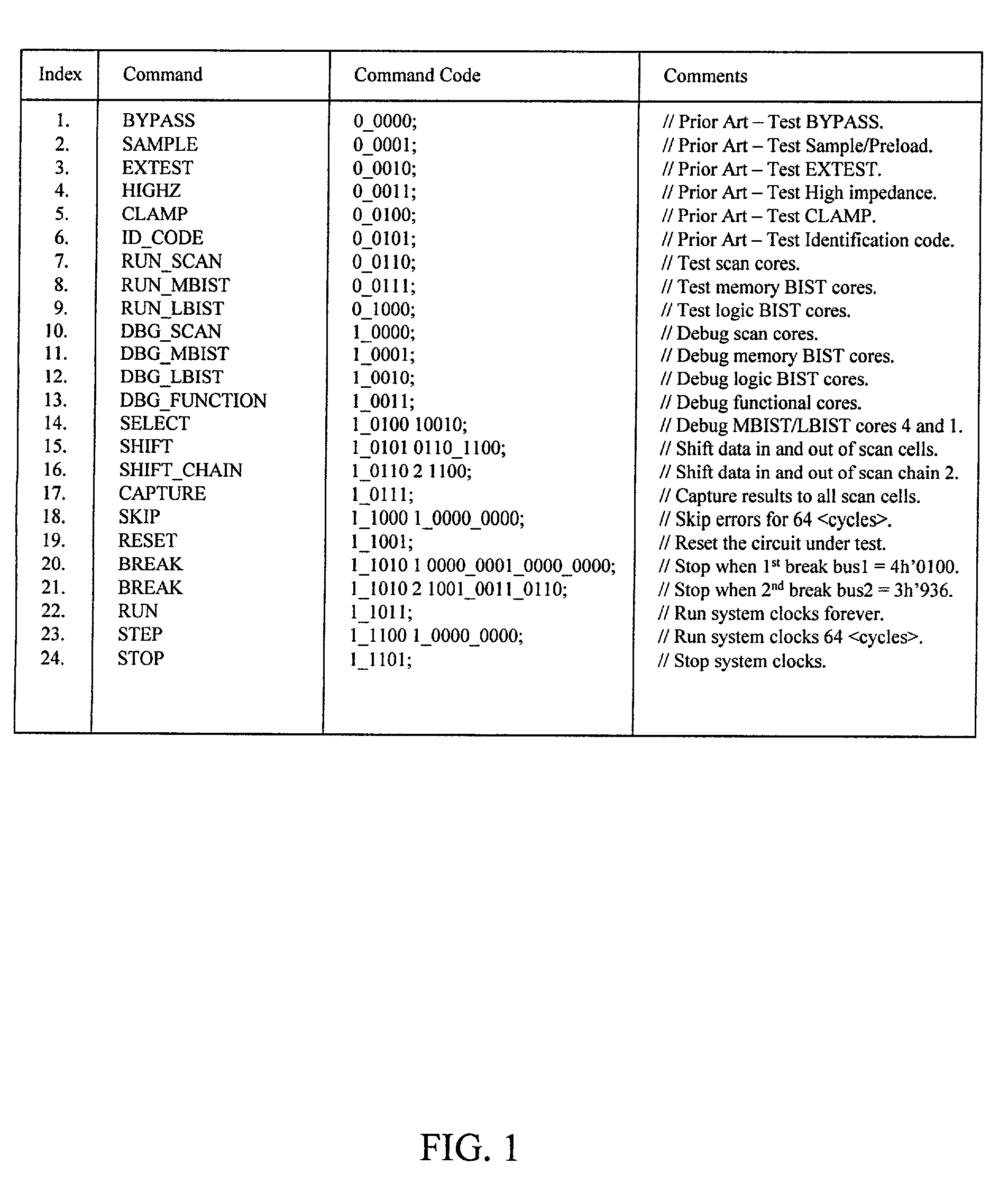
[0009]In one aspect of the present invention, the method provides a basic set of boundary-scan controlled DFD commands to test, debug, or diagnose the above-mentioned DFT modules. (Please refer to FIG. 1 in the DETAILED DESCRIPTION OF THE DRAWINGS section for further descriptions). These basic DFD commands, when used alone or combined together, will allow designers to debug DFT and functional errors on an evaluation board or system using a low-cost, boundary-scan controlled DFT debugger.
[0035]There are a number of advantages of using this seed register for logic BIST diagnosis. First, it can locate multiple signature errors. Conventional approaches without the ability of shifting selected seed to the failed BIST cycle could only find the first signature error. Second, it can further locate multiple errors in scan chains and scan cells. Finally, linear search or binary search can be employed alone or combined together to reduce diagnosis time.

Problems solved by technology

However, it is becoming more and more difficult to guarantee that the integrated circuit, even embedded with DFT circuitries, will function the first time.
This process is tedious and time-consuming, as it requires collaborative efforts between design engineers and test engineers, and heavily relies on the tester's availability.
While these approaches can eventually identify physical failures in the integrated circuit, it is still highly possible that the chip won't work on an evaluation board or system due to undiscovered timing errors on the ATE or missing functional specification.
This missing link between DFT verification on an ATE and functional verification on an evaluation board or system could potentially miss the chip's time-to-market or time-to-volume window.

Method used


Image

  • Method and apparatus for diagnosing failures in an integrated circuit using design-for-debug (DFD) techniques
  • Method and apparatus for diagnosing failures in an integrated circuit using design-for-debug (DFD) techniques
  • Method and apparatus for diagnosing failures in an integrated circuit using design-for-debug (DFD) techniques

Examples


first embodiment

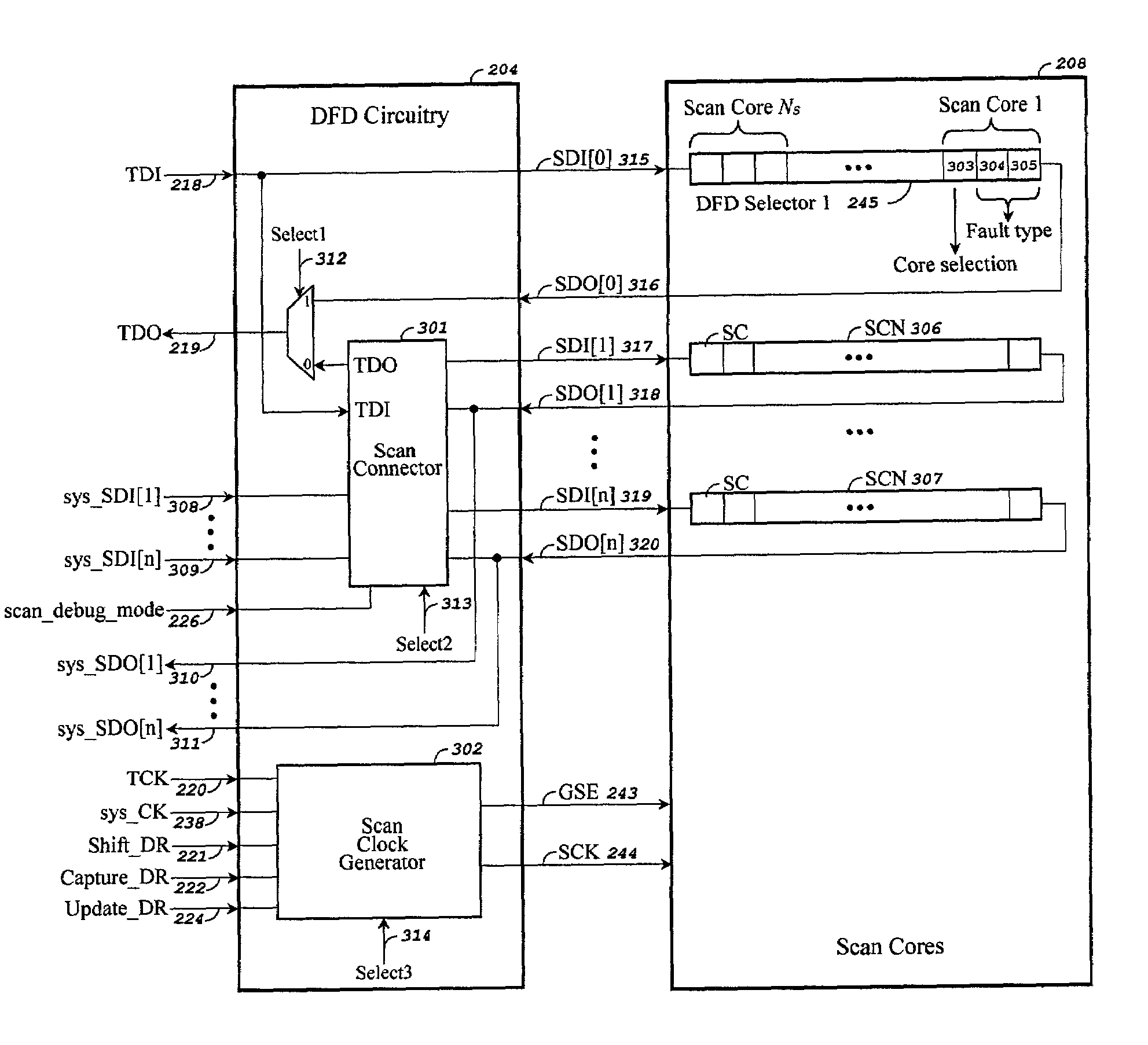
[0090]FIG. 4 shows a scan connector 408 of the present invention to stitch multiple scan chains SCN 409 to 412 to one serial scan chain SSC 414 for the purpose of diagnosing scan cores 208, logic BIST cores 210, or functional cores 211.

[0091]The scan chain SCN 409 is driven by the scan clock SCK[1]416, the scan chains SCN 410 and 411 are in the same clock domain driven by the scan clock SCK[2]419, and the scan chain SCN 412 is driven by the scan clock SCK[3]424. With four multiplexers 402 to 406 in the scan connector 408, the four scan chains 409 to 412 are stitched into one serial scan chain SSC 414. The Select5426 signal should be generated so that all scan chains SCN 409 to 412 get input data from TDI 218 in debug mode and from the external scan data inputs sys_SDI[1]415, sys_SDI[2]418, sys_SDI[3]421, and sys_SDI[4]423 in test mode. The Select4435 signal should be generated so that the boundary-scan chain BSC 401, the serial scan chain SSC 414, or other registers can be properly ...

second embodiment

[0093]FIG. 5 shows a scan connector of the present invention to stitch multiple scan chains to one serial scan chain for diagnosing scan cores 208, logic BIST cores 210, or functional cores 211.

[0094]In FIG. 5(a), the serial scan chain SSC 501, formed in the way shown in FIG. 4, is placed before the boundary-scan chain BSC 502. The Select6503 and Select7504 signals should be generated so that the boundary-scan chain BSC 502, the combined scan chain composed of the serial scan chain SSC 501 and the boundary-scan chain BSC 502, or other registers can be properly placed between TDI 218 and TDO 219 according to various test and debug requirements.

[0095]In FIG. 5(b), the serial scan chain SSC 506, formed in the way shown in FIG. 4, is placed after the boundary-scan chain BSC 505. The Select8507 signal should be generated so that the boundary-scan chain BSC 505, the combined scan chain composed of the boundary-scan chain BSC 505 and the serial scan chain SSC 506, or other registers can be...

third embodiment

[0096]FIG. 6 shows a scan connector 606 of the present invention to stitch multiple scan chains SCN 607 to 610 to a plurality of grouped scan chains GSC 612 for diagnosing scan cores 208, logic BIST cores 210, or functional cores 211.

[0097]The scan chain SCN 607 is driven by the scan clock SCK[1]614, the scan chains SCN 608 and 609 are in the same clock domain driven by the scan clock SCK[2]617, and the scan chain SCN 610 is driven by the scan clock SCK[3]622. With four multiplexers 602 to 605 in the scan connector 606, the four scan chains SCN 607 to 610 are stitched into three groups: the scan chain SCN 607 being in the first group, the scan chains SCN 608 and 609 being in the second group, and the scan chain SCN 610 being in the third group. The Select9624 signal should be generated so that all scan chains SCN 607 to 610 get input data from TDI 218 in debug mode and from the external scan data inputs sys_SDI[1]613, sys_SDI[2]616, sys_SDI[3]619, and sys_SDI[4]621 in test mode. The...


PUM


Abstract

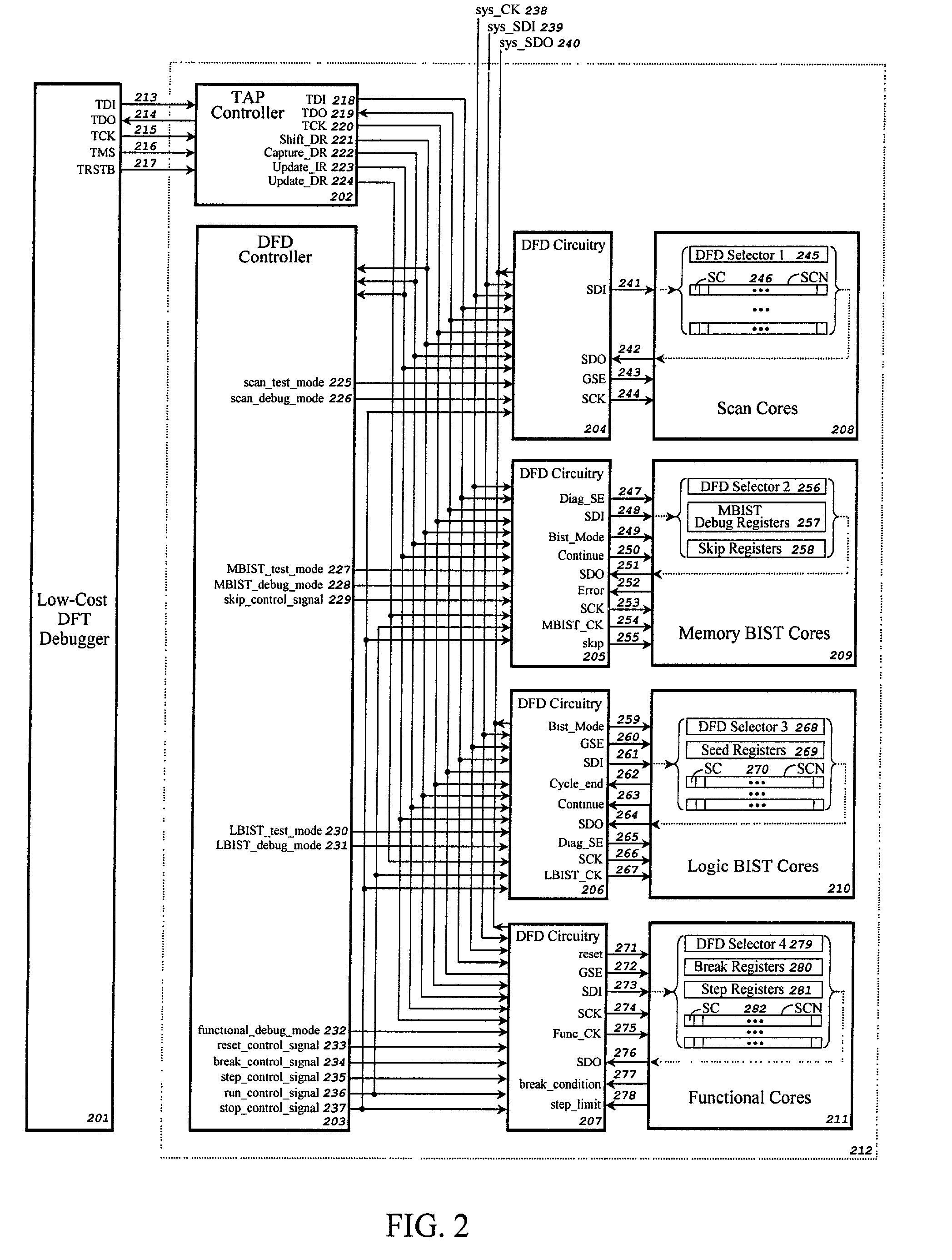
A method and apparatus for inserting design-for-debug (DFD) circuitries in an integrated circuit to debug or diagnose DFT modules, including scan cores, memory BIST (built-in self-test) cores, logic BIST cores, and functional cores. The invention further comprises using a DFD controller for executing a plurality of DFD commands to debug or diagnosis the DFT modules embedded with the DFD circuitries. When used alone or combined together, these DFD commands will detect or locate physical failures in the DFT modules in the integrated circuit on an evaluation board or system using a low-cost DFT debugger. A computer-aided design (CAD) method is further developed to synthesize the DFD controller and DFD circuitries according to the IEEE 1149.1 Boundary-scan Std. The DFD controller supports, but is not limited to, the following DFD commands: RUN_SCAN, RUN_MBIST, RUN_LBIST, DBG_SCAN, DBG_MBIST, DBG_LBIST, DBG_FUNCTION, SELECT, SHIFT, SHIFT_CHAIN, CAPTURE, RESET, BREAK, RUN, STEP, and STOP.

Description

RELATED APPLICATION DATA[0001]This application claims the benefit of U.S. Provisional Application No. 60 / 272,064 filed Mar. 1, 2001, titled “A Computer-Aided Design System for Automatic Synthesis of Design for Debug Circuitry with Boundary-Scan in Scan-Based Integrated Circuits”, which is hereby incorporated by reference.TECHNICAL FIELD[0002]The present invention generally relates to the testing, debugging, and diagnosis of integrated circuits embedded with design-for-test (DFT) and design-for-debug (DFD) techniques. Specifically, the present invention relates to prototype debug or fault diagnosis using DFT and DFD techniques to debug or diagnose physical failures in an integrated circuit.BACKGROUND[0003]Recent advance in semiconductor manufacturing and design-for-test (DFT) technology has produced very high-quality integrated circuits containing millions of gates. The most popular DFT techniques used to-date in an integrated circuit include scan, memory BIST (built-in self-test), l...

Claims


Application Information

Patent Timeline
IPC IPC(8): G01R31/28G01R31/317G01R31/3185
CPCG01R31/31704G01R31/3185G01R31/31705
Inventor WANG, LAUNG-TERNG L.-T.CHANG, MING-TUNGLIN, SHYH-HORNGCHAO, HAO-JANLEE, JAEHEEWANG, HSIN-POWEN, XIAOQINGHSU, PO-CHINGKAO, SHIH-CHIALIN, MENG-CHYITSAI, SEN-WEIHSU, CHI-CHAN
Owner SYNTEST TECH
Learn More