Non-volatile memory and method with peak current control

a non-volatile memory and peak current technology, applied in static storage, digital storage, instruments, etc., can solve the problems of unsuitable mobile and handheld environment, bulky disk drives, and easy mechanical failure,

Active Publication Date: 2014-10-07
SANDISK TECH LLC
View PDF18 Cites 4 Cited by
  • Summary
  • Abstract
  • Description
  • Claims
  • Application Information

AI Technical Summary

Benefits of technology

[0002]Solid-state memory capable of nonvolatile storage of charge, particularly in the form of EEPROM and flash EEPROM packaged as a small form factor card, has become the storage of choice in a variety of mobile and handheld devices, notably information appliances and consumer electronics products. Unlike RAM (random access memory) that is also solid-state memory, flash memory is non-volatile, and retaining its stored data even after power is turned off. Also, unlike ROM (read only memory), flash memory is rewritable similar to a disk storage device. In spite of the higher cost, flash memory is increasingly being used in mass storage applications. More recently, flash memory in the form of solid-state disks (“SSD”) is beginning to replace hard disks in portable computers as well as in fixed location installations. Conventional mass storage, based on rotating magnetic medium such as hard drives and floppy disks, is unsuitable for the mobile and handheld environment. This is because disk drives tend to be bulky, are prone to mechanical failure and have high latency and high power requirements. These undesirable attributes make disk-based storage impractical in most mobile and portable applications. On the other hand, flash memory, both embedded and in the form of a removable card or SSD are ideally suited in the mobile and handheld environment because of its small size, low power consumption, high speed and high reliability features.
[0014]U.S. Pat. No. 7,701,764 discloses limiting the number of simultaneous operating chips. These spikes are predictable to some extend since they correlate with operations that are determined by the internal state-machine (e.g. pre-charging the bit-lines prior to programming). When a global memory command is received at each chip concurrently, it is initiated at different times for at least two of the chips to mitigate peak power consumption.
[0017]Thus, the various solutions are to have the start times of the individual operations of each die staggered (skewed). This can prevent alignment of peak current at the beginning of any sequence. However, for long operation sequences which have internally timed state-machines, the die may start to un-skew and re-align.
[0018]In yet another solution, the programming operation has step-by-step start / stop control (“Peak Current Control”). This allows for an external controller to have fine-grained control over start of individual phases of the programming algorithm so as to maintain the skew over the long run. This puts extra control burden on an external controller.
[0019]Thus, there is a need to provide a nonvolatile memory that can efficiently allow multiple dice or chips to operate in parallel without exceeding the power capacity of the memory.SUMMARY OF THE INVENTION
[0028]In general, the multiple dice power management does not require the involvement of a memory controller. Only one pin is required for each die to interact with the load signal bus. In this way, a memory device can manage the budget of the power needed for parallel operations among its multiple dice without an external controller.

Problems solved by technology

Conventional mass storage, based on rotating magnetic medium such as hard drives and floppy disks, is unsuitable for the mobile and handheld environment.
This is because disk drives tend to be bulky, are prone to mechanical failure and have high latency and high power requirements.
These undesirable attributes make disk-based storage impractical in most mobile and portable applications.
Obviously, the more bits a memory cell is configured to store, the smaller is the margin of error it has to operate in.
Thus the supply current (“ICC”) are liable to have large spikes due to these internal operations.
These spikes may align and violate the total package ICC allowance for peak current.
This method cannot detect the sum-up of smaller current and only one chip can be doing the peak current operation at a time.
However, for long operation sequences which have internally timed state-machines, the die may start to un-skew and re-align.
This puts extra control burden on an external controller.

Method used


Image

  • Non-volatile memory and method with peak current control
  • Non-volatile memory and method with peak current control
  • Non-volatile memory and method with peak current control

Examples


Embodiment Construction

Memory System

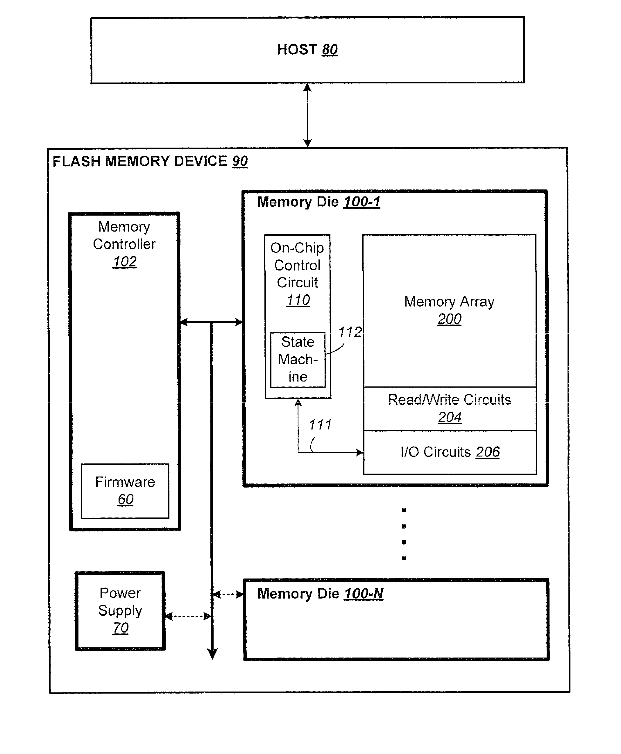
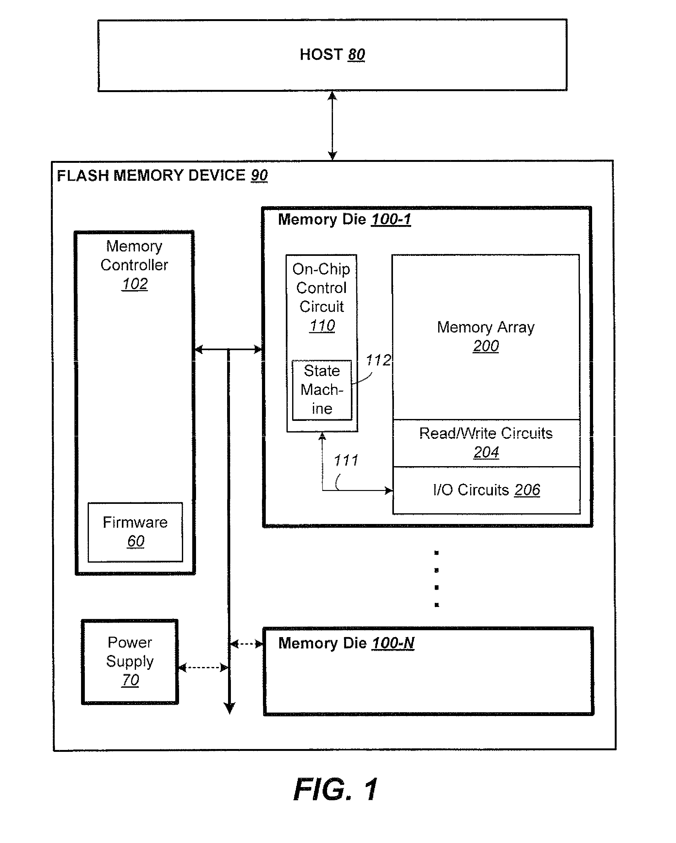
[0039]FIG. 1 illustrates a host in communication with a memory device in which the features of the present invention are embodied. The host 80 typically sends data to be stored at the memory device 90 or retrieves data by reading the memory device 90. The memory device 90 includes one or more memory die or chip 100 managed by a memory controller 102. The memory controller 102 is typically implemented as another chip. FIG. 1 shows, for example, the memory device having N die, such as memory die 100-1, . . . , memory die 100-N. The memory device 90 is powered by a power supply 70 that has a predetermined maximum capacity. A memory device bus 91 provides communications and power between the memory controller 102, the power supply 70 and the one or more memory die 100.

[0040]The memory die 100 includes a memory array 200 of memory cells with each cell capable of being configured as a multi-level cell (“MLC”) for storing multiple bits of data, as well as capable of being conf...


PUM


Abstract

A non-volatile memory with multiple memory dice manages simultaneous operations so as to not exceed a system power capacity. A load signal bus is pulled up with a strength proportional to the system power capacity. Each die has a driver to pull down the bus by an amount corresponding to its degree of power need as estimated by a state machine of the die. The bus therefore provides a load signal that serves as arbitration between the system power capacity and the cumulative loads of the individual dice. The load signal is therefore at a high state when the system power capacity is not exceeded; otherwise it is at a low state. When a die wishes to perform an operation and requests a certain amount of power, it drives the bus accordingly and its state machine either proceeds with the operation or not, depending on the load signal.

Description

[0001]This application relates to the operation of re-programmable non-volatile memory systems such as semiconductor flash memory, and, more specifically, to efficient control of peak current in a multi-die operating environment.[0002]Solid-state memory capable of nonvolatile storage of charge, particularly in the form of EEPROM and flash EEPROM packaged as a small form factor card, has become the storage of choice in a variety of mobile and handheld devices, notably information appliances and consumer electronics products. Unlike RAM (random access memory) that is also solid-state memory, flash memory is non-volatile, and retaining its stored data even after power is turned off. Also, unlike ROM (read only memory), flash memory is rewritable similar to a disk storage device. In spite of the higher cost, flash memory is increasingly being used in mass storage applications. More recently, flash memory in the form of solid-state disks (“SSD”) is beginning to replace hard disks in port...

Claims


Application Information

Patent Timeline
Patent Type & Authority Patents(United States)
IPC IPC(8): G11C7/00
CPCG11C5/14G11C16/30
Inventor LEE, DANACHEN, YI-CHIEHMOOGAT, FAROOKH
Owner SANDISK TECH LLC
Why Eureka
Try Eureka