Semiconductor device and manufacturing method thereof

a technology of semiconductor devices and manufacturing methods, applied in semiconductor devices, semiconductor/solid-state device details, electrical apparatus, etc., can solve the problems of affecting the quality of the product, and the inability to form the desired position of the wiring with satisfactory accuracy, so as to achieve satisfactory accuracy, suppress the effect of product yield degradation and satisfactory accuracy

Inactive Publication Date: 2007-03-20
LAPIS SEMICON CO LTD
View PDF5 Cites 24 Cited by
  • Summary
  • Abstract
  • Description
  • Claims
  • Application Information

AI Technical Summary

Benefits of technology

[0019]Therefore, it is a principal object of the present invention to provide a semiconductor device having a high reliable fan-out structure capable of relaxing an interval (pitch) between external terminals, and a manufacturing method thereof.
[0037]As a result, since a mounting surface on which the external terminals are disposed, is made wide, it is possible to relax narrowing of an array pitch between the external terminals with the scaling down of the semiconductor chip. Thus, since the difficulty of routing wirings extending from the electrode pads to the external terminals is relaxed, degradation in product yield can be suppressed.
[0038]Further, according to the present configuration, since the semiconductor chips can be mounted so as to extend along first target lines (or called also reference lines) formed in the mounting substrate, the semiconductor chips can be mounted with satisfactory accuracy as compared with the case in which the semiconductor chips are mounted without using the target lines.
[0039]Thus, since the semiconductor chip can be mounted to a design desired position with satisfactory accuracy, each wiring can be formed at its desired position with satisfactory accuracy upon-formation of the wiring after its mounting, thus making it possible to suppress degradation in product yield.
[0040]Further, according to the present configuration, trenches that function as target lines carry out even the function of improving adhesion between the encapsulating layer and the semiconductor chip. Thus, in the semiconductor devices individualized via the fractionizing process, the encapsulating layer can be prevented from being peeled from the surface of each semiconductor chip.

Problems solved by technology

In the WCSP having such a fan-in structure, the number of external terminals capable of being disposed on the mounting surface is limited.
As a result, there has been fear that since the routing of wirings from the electrode pads on the semiconductor chip to the external terminals narrow in array pitch becomes complicated, degradation in product yield and the like occur.
It was, however, difficult to form a wiring in desired position with satisfactory accuracy in the case of the formation of the wiring subsequent to a resin encapsulating process in each WCSP described up to now.
This is because it is difficult to control with satisfactory accuracy as designed, the relationship of layout between the position of a mask pattern for patterning the wiring and the positions of plural semiconductor chips.

Method used


Image

  • Semiconductor device and manufacturing method thereof
  • Semiconductor device and manufacturing method thereof
  • Semiconductor device and manufacturing method thereof

Examples


Embodiment Construction

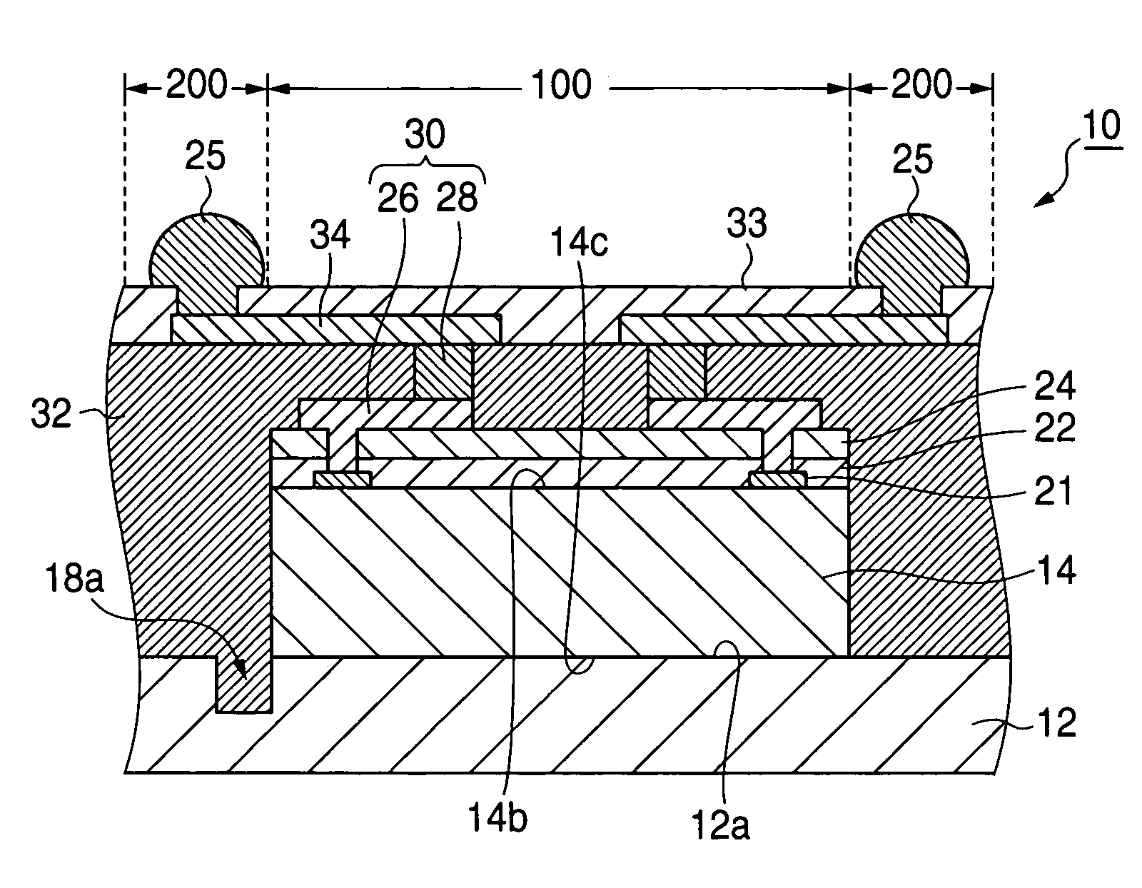
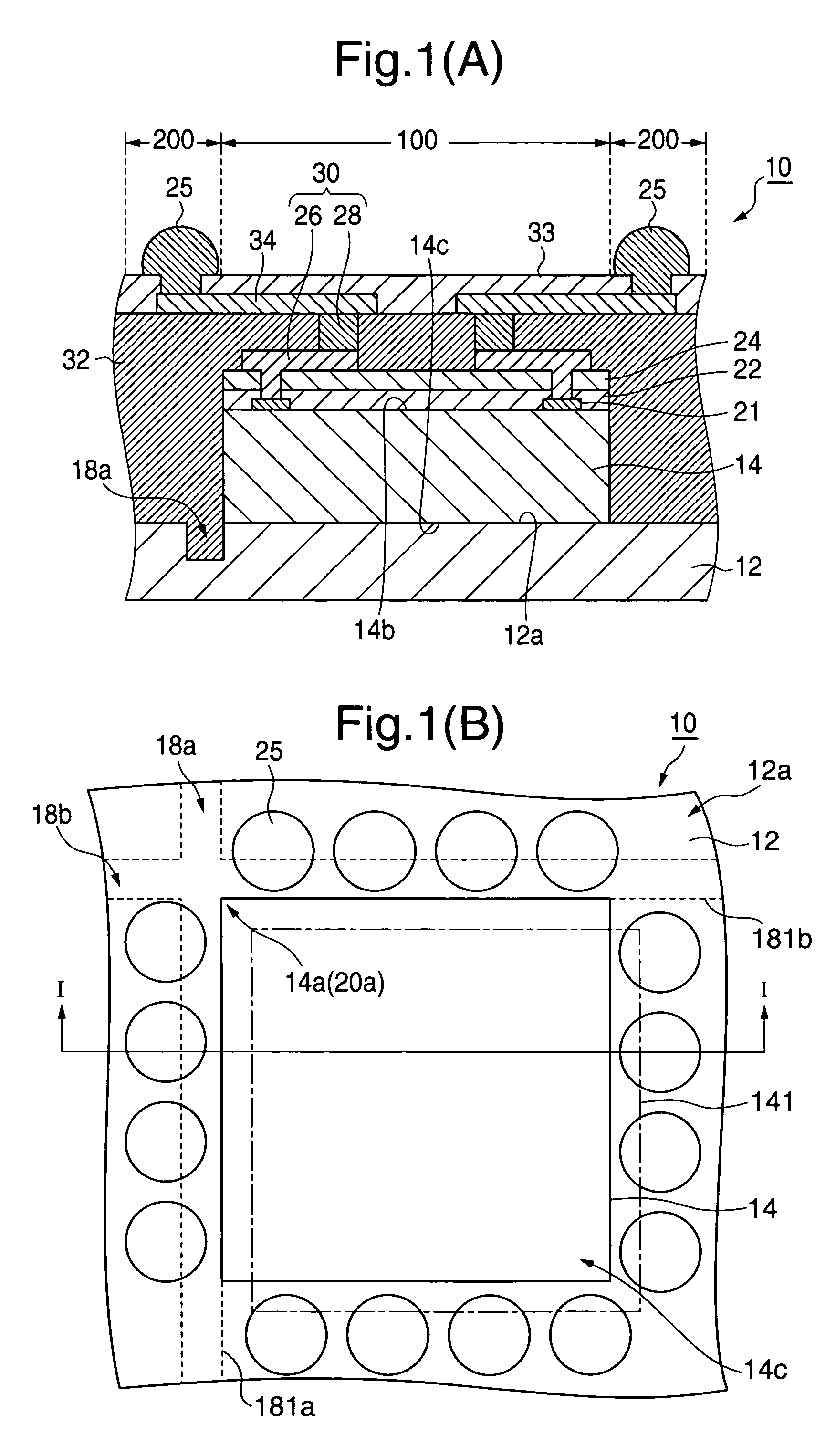
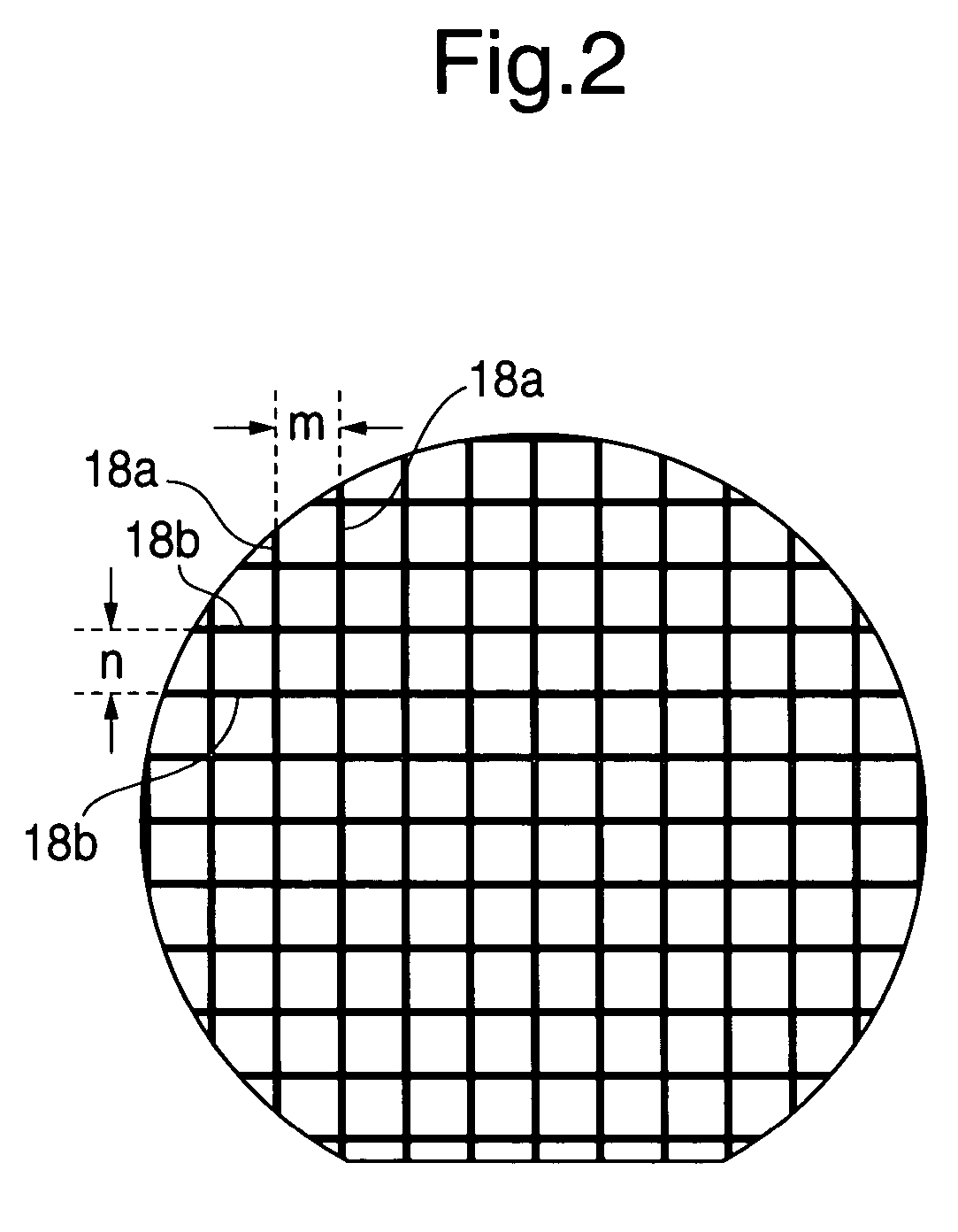
[0048]Embodiments of the present invention will be described hereinbelow with reference to the accompanying drawings. Incidentally, the respective drawings merely roughly show the sizes, shapes and positional relationships of respective components to such a degree that the present invention can be understood. Accordingly, the present invention is not limited to the illustrated embodiments. In order to make it easy to understand the drawings, hatching for showing sections are omitted except for parts. Incidentally, the embodiments described below are simply preferred examples and illustrated numerical conditions are by no means limited to these. In the respective drawings, similar components are respectively identified by the same reference numerals and the description of common components might be omitted.

[0049]A semiconductor device according to an embodiment of the present invention and a manufacturing method thereof will be explained with reference to FIGS. 1 through 6. FIG. 1(A)...


PUM


Abstract

A plurality of semiconductor chips (14) each having a first main surface (14b) formed with electrode pads (21) and a second main surface (14c) opposite to the first main surface are respectively mounted on a chip mounting surface (12a) larger in area than the second main surface, of a wafer-shaped mounting substrate (12) at equal intervals so as to extend along first and second trenches (18a, 18b) defined in the chip mounting surface with these trenches as target lines. Thereafter, solder balls (25) electrically connected to the electrode pads of the semiconductor chips are disposed on their corresponding wiring patterns 34 that extend from above first regions (100) located above the semiconductor chips, of a surface region of an encapsulating layer (32) covering the semiconductor chips to above second regions (200) that surround the first regions. Afterwards, the encapsulating layer and the mounting substrate are cut and thereby fractionized into semiconductor devices each having a fan-out structure.

Description

BACKGROUND OF THE INVENTION[0001]1. Field of the Invention[0002]The present invention relates to a semiconductor device having a fan-out structure and a manufacturing method thereof.[0003]This application is counterpart of Japanese patent application, Serial Number 399373 / 2003, filed Nov. 28, 2003, the subject matter of which is incorporated herein by reference.[0004]2. Description of the Related Art[0005]The need to scale down and thin an outer size (package size) of a semiconductor device mounted to an electronic equipment such as a portable device has been increasing in recent years. With its demand, there has been proposed a CSP (Chip Size Package) corresponding to a semiconductor device on which packaging is effected in substantially the same outer size as an outer size of a semiconductor chip.[0006]In terms of a reduction in manufacturing cost, attention is now given, as one form of CSP, to a WCSP (Waferlevel Chip Size Package) obtained by fractionization by use of dicing or t...

Claims


Application Information

Patent Timeline
Patent Type & Authority Patents(United States)
IPC IPC(8): H01L23/02H01L21/3205H01L23/52H01L21/56H01L23/12H01L23/13H01L23/31H01L23/538
CPCH01L23/13H01L23/5389H01L24/19H01L23/3114H01L2924/01033H01L2224/04105H01L2224/20H01L2224/211H01L2924/01013H01L2924/01029H01L2924/01078H01L2924/01082H01L2924/15311H01L2924/01005H01L2924/01006H01L2924/01019H01L2224/023H01L2224/73267H01L2224/83129H01L2224/32225H01L2224/92244H01L2224/12105H01L2924/0001
Inventor YAMAGUCHI, TADASHI
Owner LAPIS SEMICON CO LTD
Why Eureka
Try Eureka