Overmolded optical package

a technology of optical semiconductor and overmolded, which is applied in the direction of semiconductor devices, semiconductor/solid-state device details, electrical apparatus, etc., can solve the problems of long delivery lead times, increased cost of substrate b>12/b>, and long lead times of multi-layer ceramic substrates, etc., to achieve the effect of reducing the cost of substrates and reducing the cost of optical semiconductor packages

Inactive Publication Date: 2007-04-03
ADVANCED SEMICON ENG INC
View PDF10 Cites 59 Cited by
  • Summary
  • Abstract
  • Description
  • Claims
  • Application Information

AI Technical Summary

Benefits of technology

[0007]It is an object of the present invention to provide an optical package with a planar substrate for mass-producing and reducing the manufacturing cost.
[0009]Accordingly, the substrate of the optical semiconductor package does not have to be provided with a cavity for receiving the chip, so the substrate can be substantially planar and be an organic laminate or ceramic substrate such that the cost of the substrate is substantially reduced. Furthermore, according to the manufacturing processes of the present invention, the substrate in matrix array can be utilized for mass production and the cost of the optical semiconductor package can be further reduced.

Problems solved by technology

However, the multilayer ceramic substrate 12 has long delivery lead times and is substantially expensive.
Therefore, the cost of the substrate 12 is further increased.

Method used


Image

  • Overmolded optical package
  • Overmolded optical package
  • Overmolded optical package

Examples


Embodiment Construction

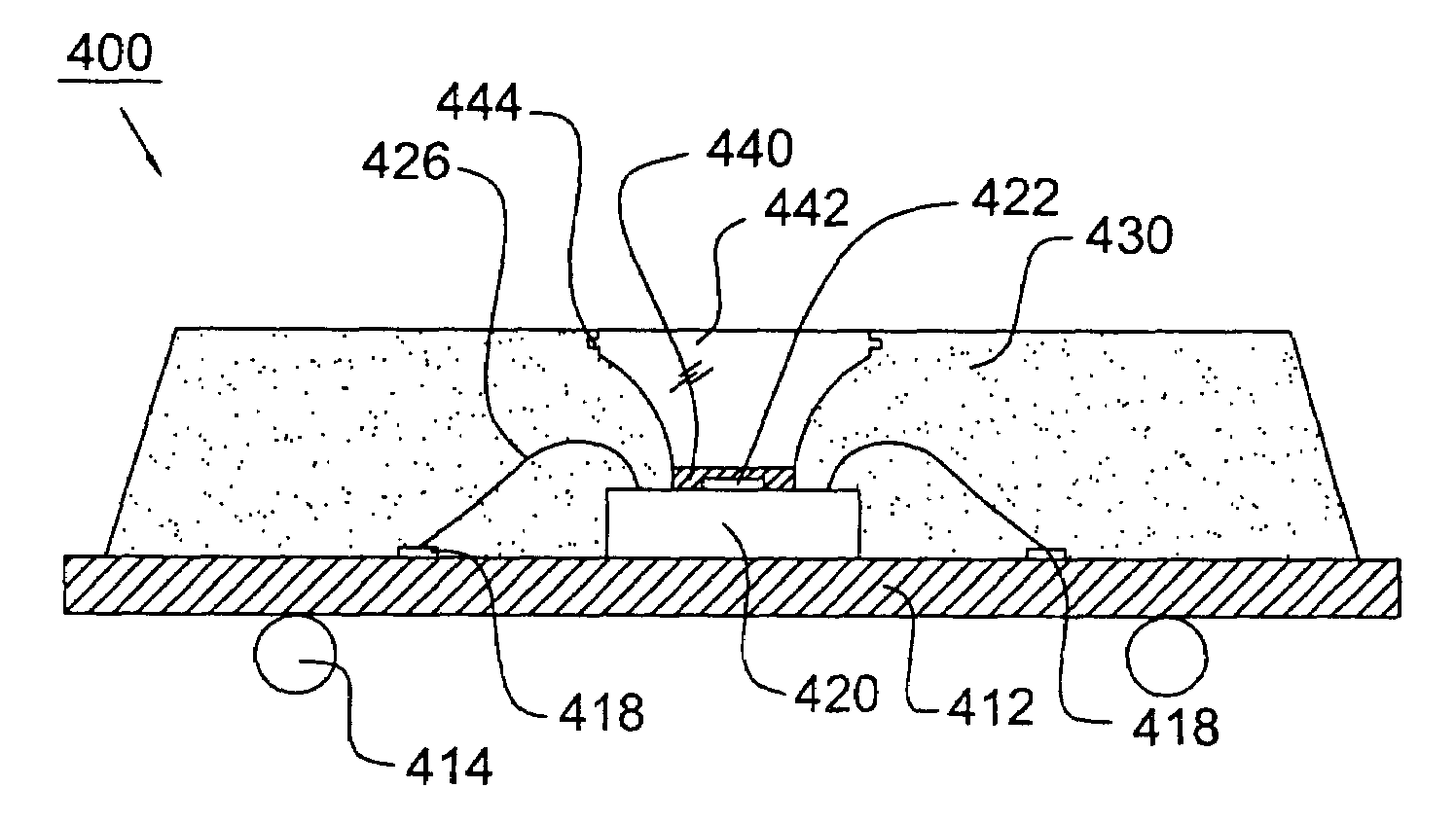
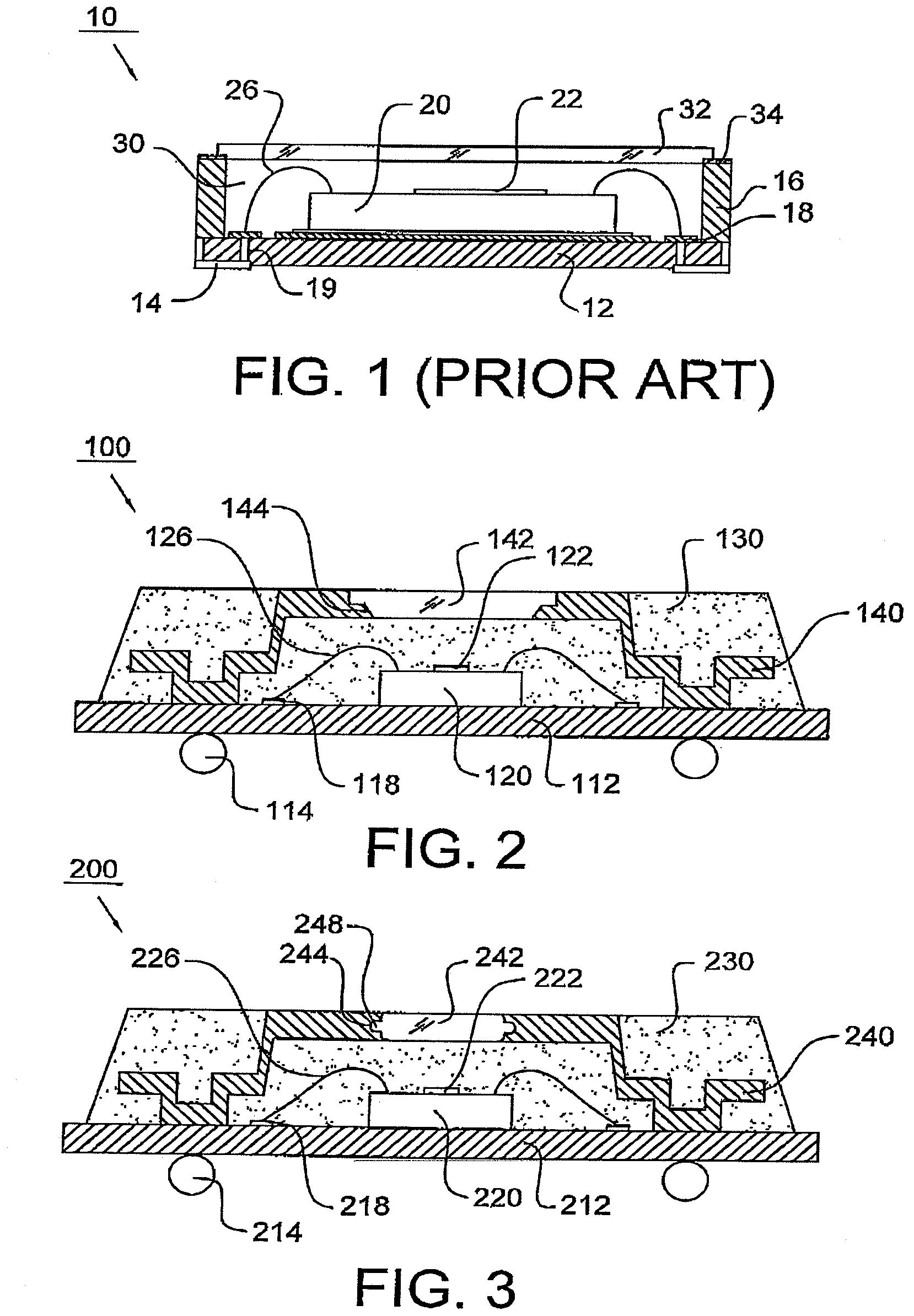
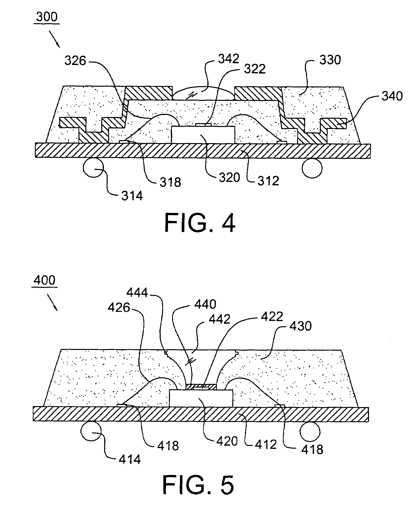
[0017]Referring to FIG. 2, it depicts an optical package 100 according to an embodiment of the present invention. The optical semiconductor package 100 comprises a carrier or substrate 112 which is substantially planar and a chip 120 mounted on the substrate 112. The substrate 112 can be either an organic laminate or a ceramic substrate. The chip 120 has optical elements 122, such as optical sensors or imaging sensors, and is electrically connected to a plurality of bonding pads 118 of the substrate 112 by a plurality of bonding wires 126. The substrate 112 is further provided with solder balls 114 electrically connected to the bonding pads 118 for being electrically connected to an external printing circuit board (not shown).

[0018]A supporter 140 is disposed on the substrate 112 and is provided with a shoulder 144 for supporting and holding a window 142. Then, an encapsulant 130 is formed by overmolding or insert molding process and the window 142 is kept in place. The window 142 i...


PUM


Abstract

An optical semiconductor package includes a substrate, a chip, a plurality of bonding wires, a window, a supporter, and an encapsulant. The chip is disposed on the substrate and has an optical element. The bonding wires are used for electrically connecting the chip to the substrate. The window is supported on the supporter and positioned over the optical element of the chip. The encapsulant is overmolded on the substrate for fixing the window and encapsulating the chip and the bonding wires.

Description

BACKGROUND OF THE INVENTION[0001]1. Field of the Invention[0002]The present invention relates to an optical semiconductor package, and more particularly, to an optical package which is manufactured by the overmolding process.[0003]2. Description of the Related Art[0004]Referring to FIG. 1, it depicts a typically optical package 10 in prior art. The optical package 10 comprises a carrier or a substrate 12 and a chip 20 mounded on the substrate 12. The substrate 12 has a sidewall 16 which surrounds the substrate 12. A transparent lid 32 is mounted on the sidewall 16 by an adhesive 34 so as to form a hermetic cavity 30 and transmit the light interacting with the chip 20. The chip 20 has optical elements 22, such as optical sensors or imaging sensors, and is disposed in the cavity 30. The chip 20 is electrically connected to a plurality of bonding pads 18 of the substrate 12 by a plurality of bonding wires 26. The bonding pads 18 on the upper surface of the substrate 12 are electrically...

Claims


Application Information

Patent Timeline
Patent Type & Authority Patents(United States)
IPC IPC(8): H01L31/0203H01L23/02H01L23/29H01L23/433H01L31/0232
CPCH01L23/4334H01L31/0203H01L31/0232H01L2224/48227H01L24/48H01L2924/181H01L2924/1815H01L2924/00014H01L31/02325H01L2924/00012H01L2224/45099H01L2224/45015H01L2924/207
Inventor APPELT, BERND KARLCHEN, WILLIAM TZE-YOU
Owner ADVANCED SEMICON ENG INC
Why Eureka
Try Eureka