Host to FPGA interface in an in-circuit emulation system

a technology of in-circuit emulation and host, applied in the field of in-circuit emulation, can solve the problems of increasing the cost and complexity of the circuit, imposing significant limitations on the circuit layout, increasing the complexity, size, power consumption,

Inactive Publication Date: 2007-04-17
CYPRESS SEMICON CORP
View PDF12 Cites 64 Cited by
  • Summary
  • Abstract
  • Description
  • Claims
  • Application Information

AI Technical Summary

Problems solved by technology

Thus, support for the debugging instruction code and the like can increase the cost and complexity of the circuit.
This technique is in common use, but has the disadvantage of imposing significant limitations on the circuit layout to permit space and circuitry associated with the special wirebonding pads.
This increases the complexity, size, power consumption and potentially reduces the yield of the production part.
Such resources may have to be applied with every updated version of the part and may significantly impact speed, cost or flexibility in development of improved versions of the part.
Of course, providing such a probe mode requires significant design resources to design in all such probe and debug functions and associated instruction code support into the standard processor.
This, of course, increases development cost, chip complexity and chip size.

Method used


Image

  • Host to FPGA interface in an in-circuit emulation system
  • Host to FPGA interface in an in-circuit emulation system
  • Host to FPGA interface in an in-circuit emulation system

Examples


Embodiment Construction

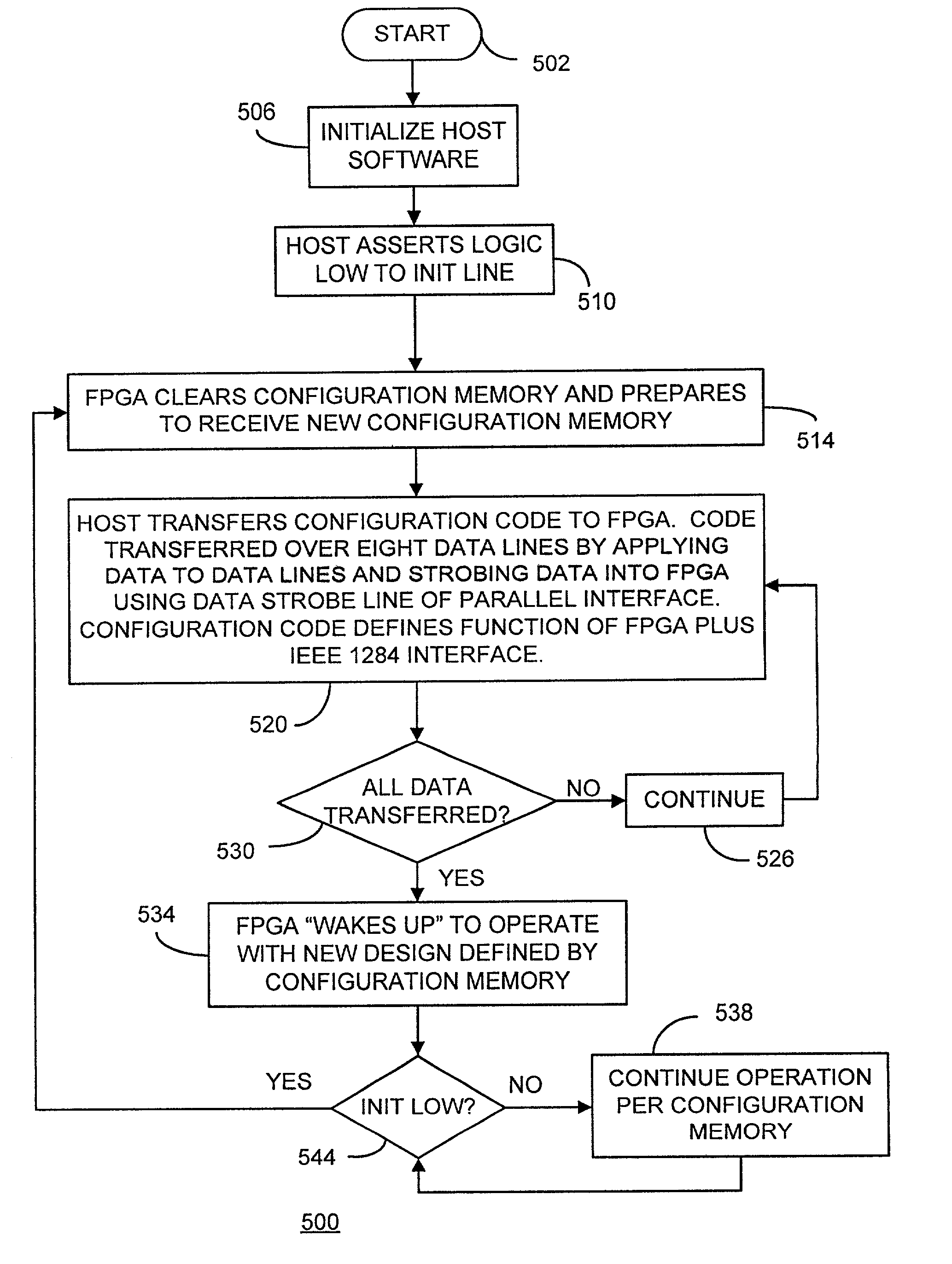
[0028]In the following detailed description of the present invention, numerous specific details are set forth in order to provide a thorough understanding of the present invention. However, it will be recognized by one skilled in the art that the present invention may be practiced without these specific details or with equivalents thereof. In other instances, well known methods, procedures, components, and circuits have not been described in detail as not to unnecessarily obscure aspects of the present invention.

Notation and Nomenclature

[0029]Some portions of the detailed descriptions which follow are presented in terms of procedures, steps, logic blocks, processing, and other symbolic representations of operations on data bits that can be performed on computer memory. These descriptions and representations are the means used by those skilled in the data processing arts to most effectively convey the substance of their work to others skilled in the art. A procedure, computer execute...


PUM


Abstract

A multi-purpose interface between a host computer and an FPGA. This interface uses an IEEE 1284 compliant EPP mode connection. When the host computer is initialized, a reset of the FPGA is carried out to clear the configuration memory of the FPGA. The data lines of the interface are then used to communicate unidirectional configuration data into the FPGA. The data are clocked by the host computer using the data strobe signal line to clock data into the FPGA. When the FPGA has been fully programmed, including programming an IEEE 1284 compliant EPP mode interface into the FPGA, the data lines are used for bidirectional communication between the host computer and the configured FPGA, in this embodiment operating as a virtual microcontroller.

Description

CROSS REFERENCE TO RELATED DOCUMENTS[0001]This application is related to U.S. patent application Ser. No. 09 / 975,115, to Warren Snyder, et al., entitled “IN-SYSTEM CHIP EMULATOR ARCHITECTURE”; and to U.S. patent application Ser. No. 09 / 975,104, to Warren Snyder, entitled “CAPTURING TEST / EMULATION AND ENABLING REAL-TIME DEBUGGING USING AN FPGA FOR IN-CIRCUIT EMULATION”; and to U.S. patent application Ser. No. 09 / 975,030, to Warren Snyder, et al., entitled “EMULATOR CHIP / BOARD ARCHITECTURE AND INTERFACE”; and to U.S. patent application Ser. No. 09 / 975,338, to Warren Snyder, et al., entitled “METHOD FOR BREAKING EXECUTION OF (TEST) CODE IN A DUT AND EMULATOR CHIP ESSENTIALLY SIMULTANEOUSLY AND HANDLING COMPLEX BREAKPOINT EVENTS”. Each of these applications is filed on the same date as the present application and is hereby incorporated by reference as though disclosed fully herein. This application is also related to and claims priority benefit under 35 U.S.C. § 119(e) of provisional pa...

Claims


Application Information

Patent Timeline
Patent Type & Authority Patents(United States)
IPC IPC(8): G06F9/455G06F13/00
CPCG06F11/3652G06F11/3656
Inventor NEMECEK, CRAIG
Owner CYPRESS SEMICON CORP
Why Eureka
Try Eureka