Plasma display panel

a technology of display panel and plasma, which is applied in the direction of discharge tube luminescnet screen, gas-filled discharge tube, address electrode, etc., can solve the problems of limited efforts to improve discharge efficiency, affecting the stability of discharge, and so as to achieve maximum discharge efficiency and ensure discharge stability. , the effect of reducing the efficiency of converting vacuum ultraviolet rays

Inactive Publication Date: 2007-04-24
SAMSUNG SDI CO LTD
View PDF103 Cites 21 Cited by
  • Summary
  • Abstract
  • Description
  • Claims
  • Application Information

AI Technical Summary

Benefits of technology

[0016]In accordance with the present invention, a plasma display panel is provided that optimizes a structure of electrodes and discharge cells that effect discharg

Problems solved by technology

However, this limits efforts at improving discharge efficiency.
However, in the PDP structured in this manner, mis-discharge along the direction that barrier ribs 121 are formed remains a problem.
However, with the use of such a matrix barrier rib structure, since all areas except for where the barrier ribs are formed a

Method used


Image

  • Plasma display panel
  • Plasma display panel
  • Plasma display panel

Examples


first embodiment

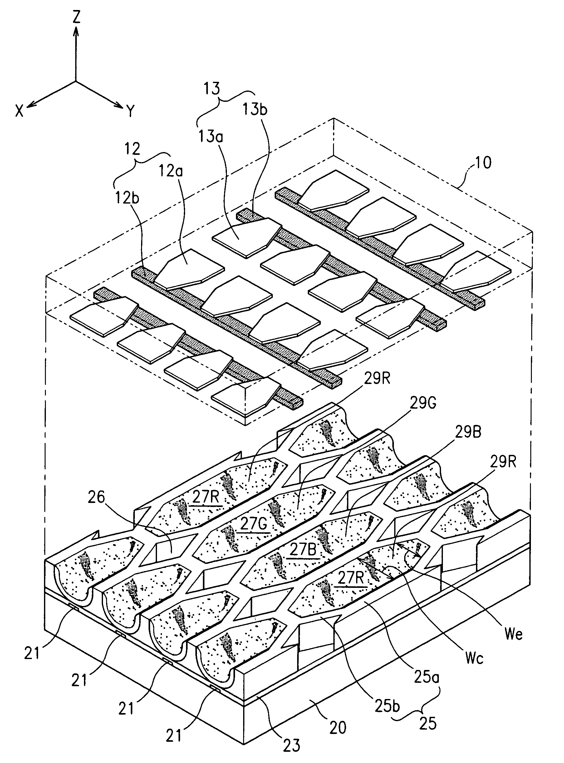
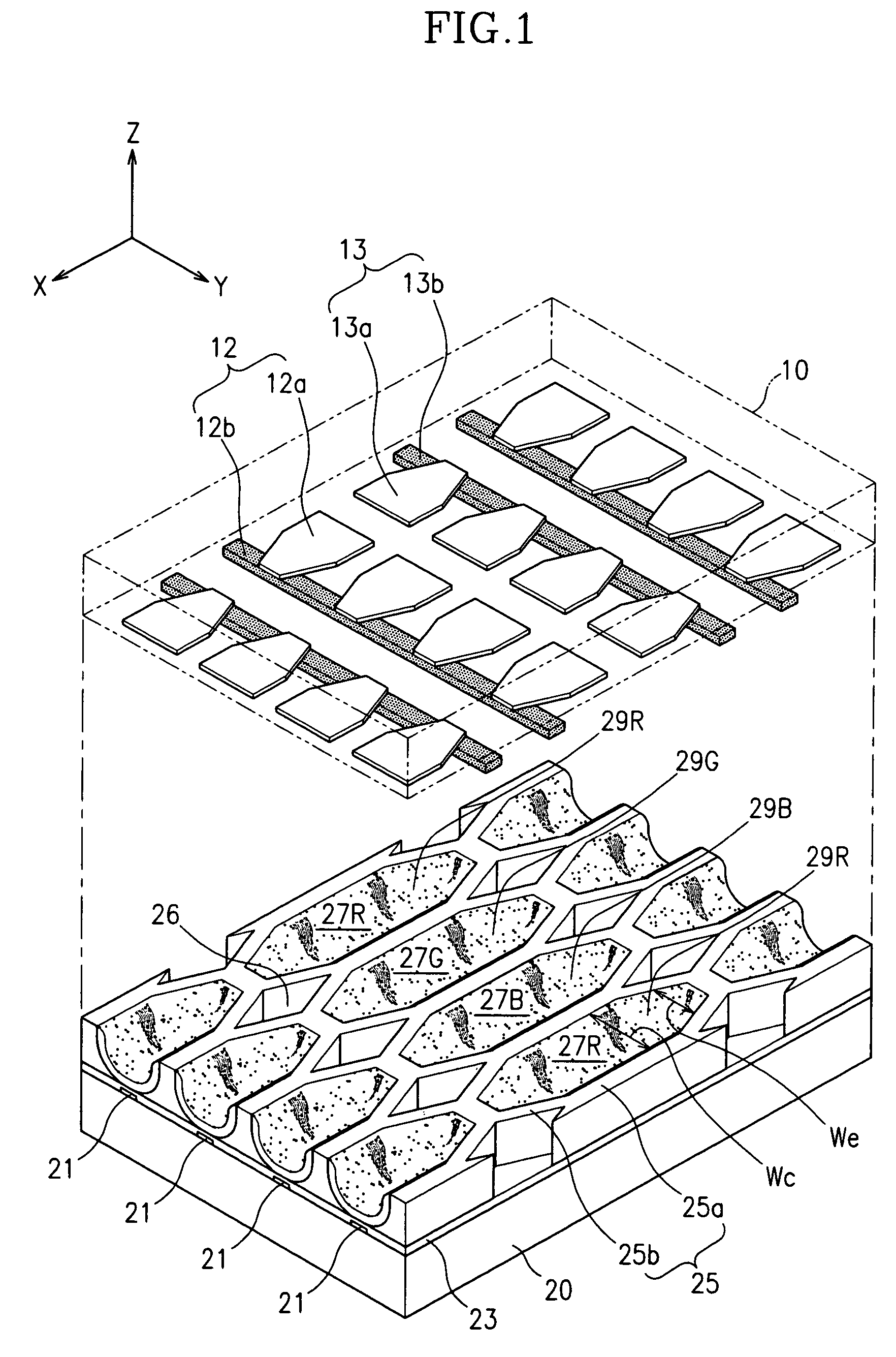
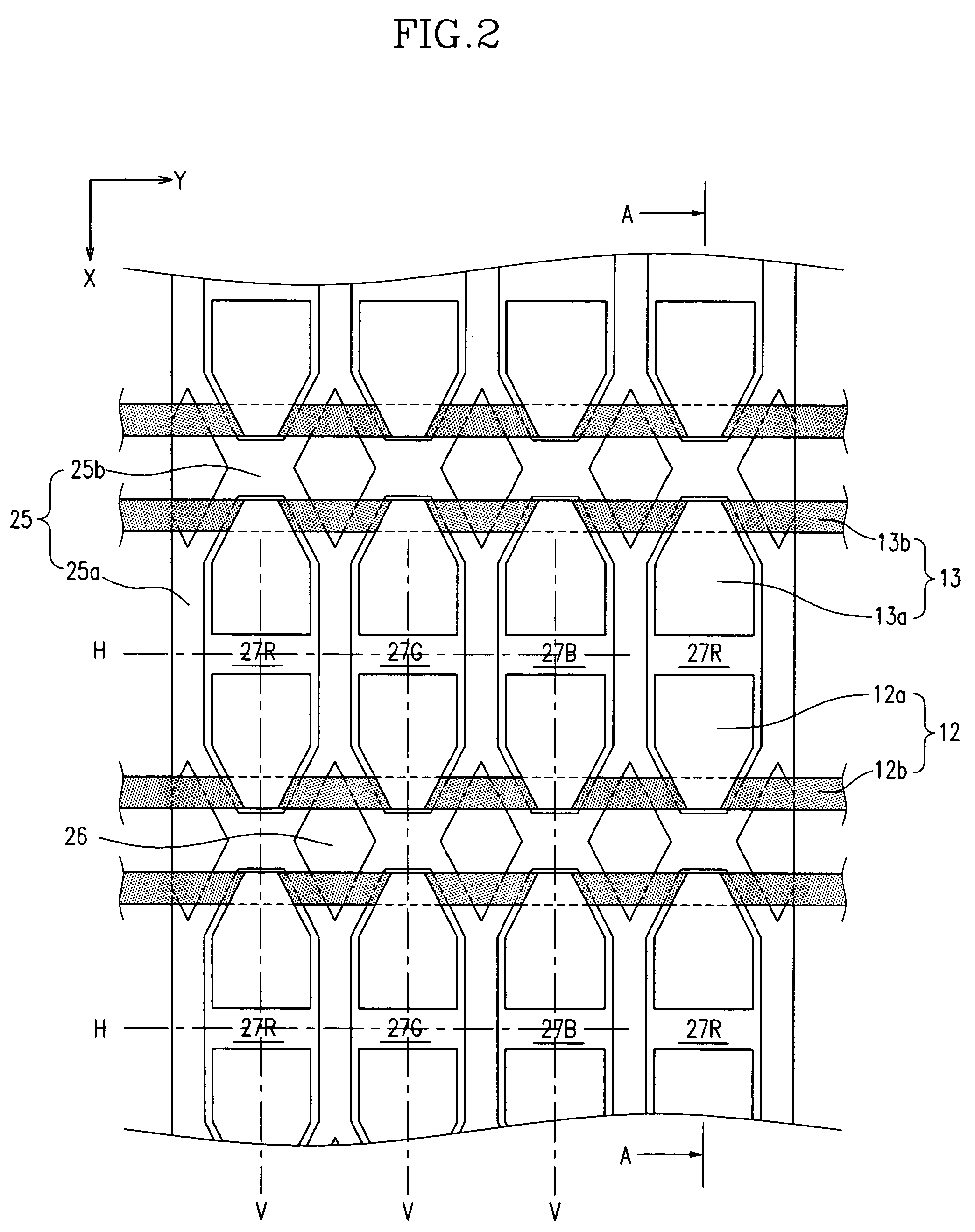
[0046]FIG. 1 is a sectional exploded perspective view of a plasma display panel according to the present invention with FIG. 2 being a partial plan view of the plasma display panel of FIG. 1.

[0047]A plasma display panel (PDP) according to the first embodiment includes first substrate 10 and second substrate 20 provided substantially in parallel with a predetermined gap therebetween. A plurality of discharge cells 27R, 27G, and 27B in which plasma discharge takes place is defined by barrier ribs 25 between first substrate 10 and second substrate 20. Discharge sustain electrodes 12 and 13 are formed on first substrate 10, and address electrodes 21 are formed on second substrate 20. This basic structure of the PDP will be described in greater detail below.

[0048]A plurality of address electrodes 21 is formed along one direction (direction X in the drawings) on a surface of second substrate 20 opposing first substrate 10. Address electrodes 21 are formed in a striped pattern with a unifo...

second embodiment

[0064]FIG. 5 is a partial plan view of a plasma display panel according to the present invention.

[0065]As shown in the drawing, in the PDP according to the second embodiment, a plurality of non-discharge regions 36 and a plurality of discharge cells 37R, 37G, and 37B are defined by barrier ribs 35. Non-discharge regions 36 are formed in areas encompassed by discharge cell abscissas and ordinates that pass through centers of each of the discharge cells 37R, 37G, and 37B, and that are aligned respectively with directions X and Y as in the first embodiment.

[0066]Ends of discharge cells 37R, 37G, and 37B are formed reducing in width in the direction of discharge sustain electrodes 17 and 18 (direction Y) as a distance from a center of each of the discharge cells 27R, 27G, and 27B is increased in the direction that address electrodes 21 are provided (direction X). Such a configuration is continued until reaching a point of minimal width such that the ends of discharge cells 37R, 37G, and...

third embodiment

[0072]FIG. 7 is a partial plan view of a plasma display panel according to the present invention.

[0073]As shown in the drawing, in the PDP according to the third embodiment, a plurality of non-discharge regions 46 and a plurality of discharge cells 47R, 47G, and 47B are defined by barrier ribs 45. Non-discharge regions 46 are formed in areas encompassed by discharge cell abscissas and ordinates that pass through centers of each of the discharge cells 47R, 47G, and 47B, and that are aligned respectively with directions X and Y as in the first embodiment. With lengths of discharge cells 47R, 47G, and 47B being provided along a direction of address electrodes 21 (direction X), ends of discharge cells 47R, 47G, and 47B are rounded into an arc shape.

[0074]Discharge sustain electrodes 12 and 13 include bus electrodes 12b and 13b, respectively, that are formed along a direction (direction Y) that is substantially perpendicular to the direction address electrodes 21 are formed (direction X)...


PUM


Abstract

A plasma display panel. A first substrate and a second substrate are provided opposing one another with a predetermined gap therebetween. Address electrodes are formed on the second substrate. Barrier ribs are mounted between the first substrate and the second substrate, the barrier ribs defining a plurality of discharge cells and a plurality of non-discharge regions. Phosphor layers are formed within each of the discharge cells. Discharge sustain electrodes are formed on the first substrate. The non-discharge regions are formed in areas encompassed by discharge cell abscissas and ordinates that pass through centers of each of the discharge cells. Further, each of the discharge cells is formed such that ends thereof increasingly decrease in width along a direction the discharge sustain electrodes are formed as a distance from a center of the discharge cells is increased along a direction the address electrodes are formed.

Description

CROSS REFERENCE TO RELATED APPLICATIONS[0001]This application claims priority to and the benefit of Korea Patent Applications No. 2003-0000088 filed on Jan. 2, 2003 and No. 2003-0045202 filed on Jul. 4, 2003, both in the Korean Intellectual Property Office, the content of which are both incorporated herein by reference.BACKGROUND OF THE INVENTION[0002](a) Field of the Invention[0003]The present invention relates to a plasma display panel (PDP), and more particularly, to a plasma display panel having a barrier rib structure between two substrates that defines discharge cells into independent units.[0004](b) Description of the Related Art[0005]A PDP is typically a display device in which ultraviolet rays generated by the discharge of gas excite phosphors to realize predetermined images. As a result of the high resolution possible with PDPs (even with large screen sizes), many believe that they will become a major, next generation flat panel display configuration.[0006]In a conventiona...

Claims


Application Information

Patent Timeline
IPC IPC(8): H01J1/62H01J17/49H01J11/12H01J11/14H01J11/22H01J11/24H01J11/26H01J11/34H01J11/36
CPCH01J11/36H01J2211/245H01J2211/365
Inventor KWON, JAE-IKKANG, KYOUNG-DOO
Owner SAMSUNG SDI CO LTD
Why Eureka
Try Eureka