
Charge pump circuit and amplifier

a charge pump and amplifier technology, applied in the direction of electric variable regulation, process and machine control, instruments, etc., can solve the problems of large voltage change at the end of the capacitor during switching, limited power supply voltage, and difficulty in using the conventional charge pump circuit in the semiconductor integrated circuit which handles an analog signal

Inactive Publication Date: 2007-04-24
SEMICON COMPONENTS IND LLC
View PDF20 Cites 22 Cited by
  • Summary
  • Abstract
  • Description
  • Claims
  • Application Information

AI Technical Summary

Benefits of technology

[0003]The present invention relates to a charge pump circuit and an amplifier which uses an output of the charge pump circuit as a power supply.
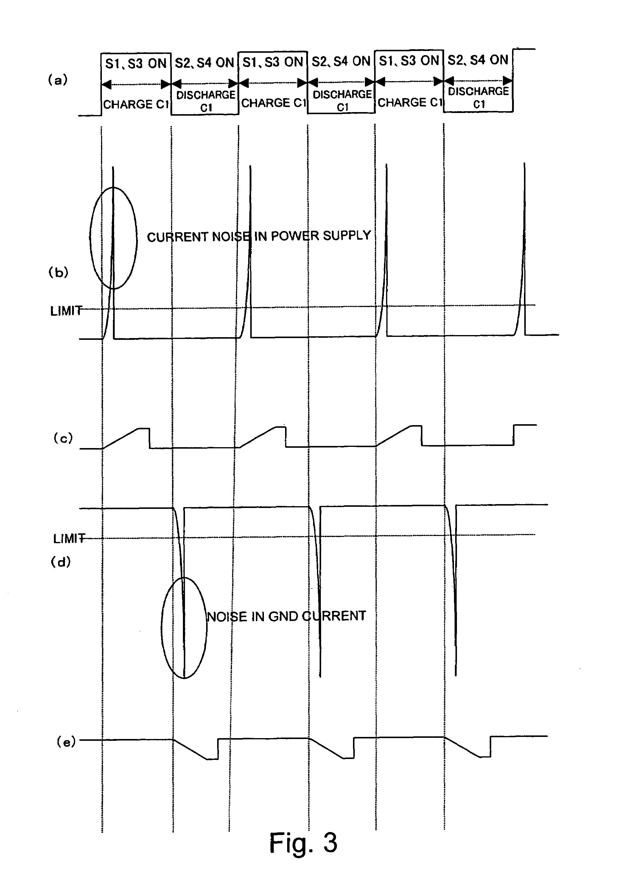
[0006]However, in the conventional charge pump circuit described above, the voltage at the end of the capacitor changes by a large amount during switching. Therefore, a large current flows to the power supply and to ground at the time of switching and noise appears at the power supply, ground, and output terminal. Although it may be possible to use the conventional charge pump circuit without a problem in a digital circuit, it is difficult to use the conventional charge pump circuit in a semiconductor integrated circuit which handles an analog signal.

Problems solved by technology

In particular, in various portable devices, because a battery power supply is used, the power supply voltage is limited.
However, in the conventional charge pump circuit described above, the voltage at the end of the capacitor changes by a large amount during switching.
Therefore, a large current flows to the power supply and to ground at the time of switching and noise appears at the power supply, ground, and output terminal.
Although it may be possible to use the conventional charge pump circuit without a problem in a digital circuit, it is difficult to use the conventional charge pump circuit in a semiconductor integrated circuit which handles an analog signal.
In a semiconductor integrated circuit, however, a current of 1 A is a large current, and when such current flows every time switching takes place, normally noise is generated.

Method used


Image

  • Charge pump circuit and amplifier
  • Charge pump circuit and amplifier
  • Charge pump circuit and amplifier

Examples


Embodiment Construction

[0025]Preferred embodiments (hereinafter referred to simply as “embodiment”) of the present invention will now be described referring to the drawings.

Charge Pump Circuit

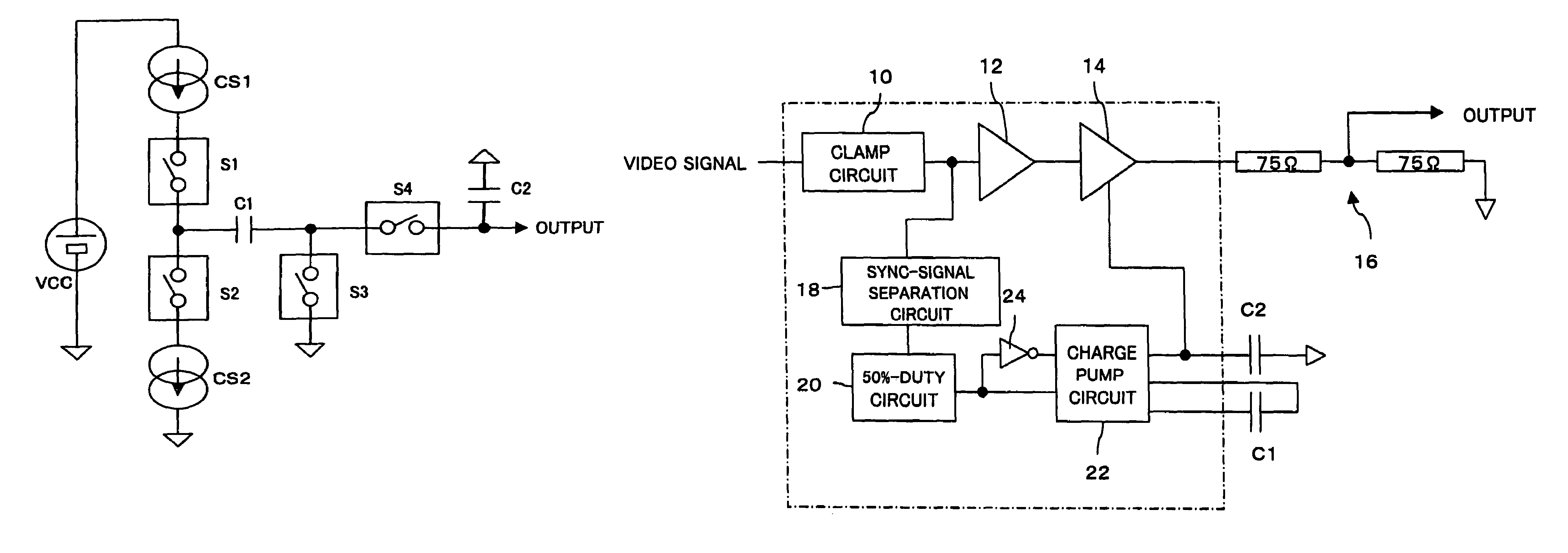
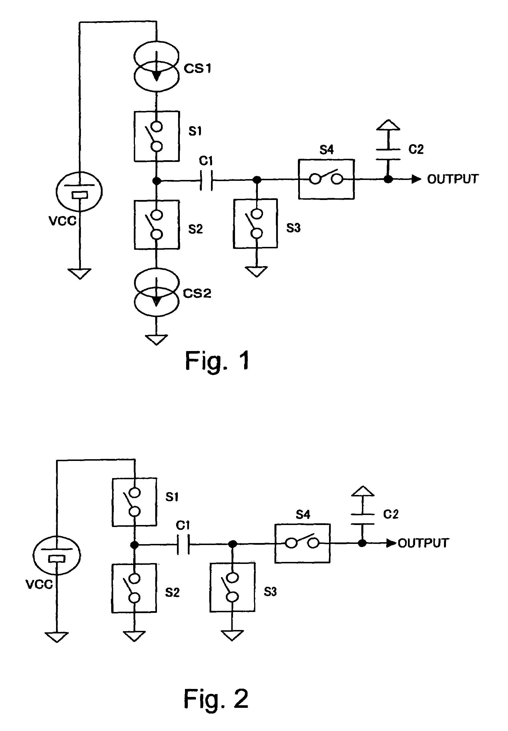
[0026]FIG. 1 is a diagram showing a structure of a charge pump circuit according to a preferred embodiment of the present invention. This circuit is also a charge pump circuit for obtaining a negative voltage −VCC from the power supply voltage VCC.

[0027]One terminal of the power supply VCC is connected to ground having a voltage of 0 V and another terminal of the power supply VCC is connected to one terminal of a capacitor C1 via a constant current circuit CS1 and a switch S1.

[0028]This terminal of the capacitor C1 is also connected to ground via a switch S2 and a constant current circuit CS2.

[0029]The other terminal of the capacitor C1 is connected to ground via a switch S3 and to an output terminal via a switch S4. In addition, one terminal of a capacitor C2 having the other terminal connected to ground is connecte...


PUM


Abstract

A charge pump circuit which uses a constant current from a constant current source for charging or discharging a capacitor and which obtains an output voltage by shifting a power supply voltage using a charged voltage of the charged capacitor. With this structure, a large current can be limited and generation of noise can be prevented.

Description

CROSS-REFERENCE TO RELATED APPLICATIONS[0001]The entire disclosure of Japanese Patent Application No. 2003-389839 including specification, claims, drawings and abstract is incorporated herein by reference.BACKGROUND OF THE INVENTION[0002]1. Field of the Invention[0003]The present invention relates to a charge pump circuit and an amplifier which uses an output of the charge pump circuit as a power supply.[0004]2. Description of the Related Art[0005]Conventionally, a charge pump circuit is used in various circuits. In particular, in various portable devices, because a battery power supply is used, the power supply voltage is limited. On the other hand, in various circuits, there is a demand to use the highest possible power supply voltage to facilitate their operations. For this purpose, a charge pump circuit is often provided to boost a voltage of the battery power supply. A charge pump circuit which uses a capacitor is disclosed in, for example, Japanese Patent Laid-Open Publication...

Claims


Application Information

Patent Timeline
Patent Type & Authority Patents(United States)
IPC IPC(8): G05F3/02H02M3/07H03F3/70
CPCH02M3/07H03F3/70H02M2001/0045H02M1/44H02M1/0045H02M3/071
Inventor HASHIMOTO, FUMINORI
Owner SEMICON COMPONENTS IND LLC
Learn More