Light emitting diodes including barrier layers/sublayers

a technology of light-emitting diodes and barrier layers, applied in semiconductor devices, semiconductor/solid-state device details, electrical apparatus, etc., can solve problems such as migration and interference with metal-semiconductor interfaces, and unwanted degradation of devices, so as to reduce the cracking of the barrier layer, and reduce the migration of metal

Inactive Publication Date: 2007-05-01
CREELED INC
View PDF89 Cites 146 Cited by
  • Summary
  • Abstract
  • Description
  • Claims
  • Application Information

AI Technical Summary

Benefits of technology

[0011]In some embodiments, the first sublayers are configured to reduce migration of metal from the reflector layer, and the second sublayers are configured to prevent at least some grain boundaries in the first sublayers for propagating thereacross. In other embodiments, the plurality of first and second alternating sublayers define first and second outer sublayers that comprise the first sublayer. In still other embodiments, the second outer sublayer is thicker than the first outer sublayer.
[0012]Other embodiments of the invention provide methods of reducing migration of metal from the reflective layer into the epitaxial region of a semiconductor light emitting device, by forming a barrier layer on the reflector layer that extends on the reflector layer sidewall. In other embodiments, the barrier layer is formed to extend on the ohmic layer sidewall. In still other embodiments, the barrier layer extends onto the epitaxial region outside the multilayer conductive stack.
[0013]Still other embodiments of the present invention form the barrier layer as a plurality of alternating first and second sublayers, which can reduce cracking of the barrier layer adjacent the reflector layer sidewall. The first and second sublayers can define an offset brick wall structure that can terminate with a first sublayer, to define an outer sublayer, wherein the second sublayers are thinner than the first sublayers and the outer sublayer is thicker than the first sublayers.

Problems solved by technology

One potential problem with flip-chip mounting is that when an LED is mounted on a submount using conventional techniques, a conductive die attach material such as silver epoxy is deposited on the LED and / or on the package, and the LED and the submount are pressed together.
However, tin (Sn) is a component of most types of solder, and migration of Sn from the bonded surface into the device can cause unwanted degradation of the device.
Such migration can interfere with metal-semiconductor interfaces such as ohmic contacts and / or the function of metal-metal interfaces such as reflective interfaces that serve as mirrors.

Method used


Image

  • Light emitting diodes including barrier layers/sublayers
  • Light emitting diodes including barrier layers/sublayers
  • Light emitting diodes including barrier layers/sublayers

Examples


Embodiment Construction

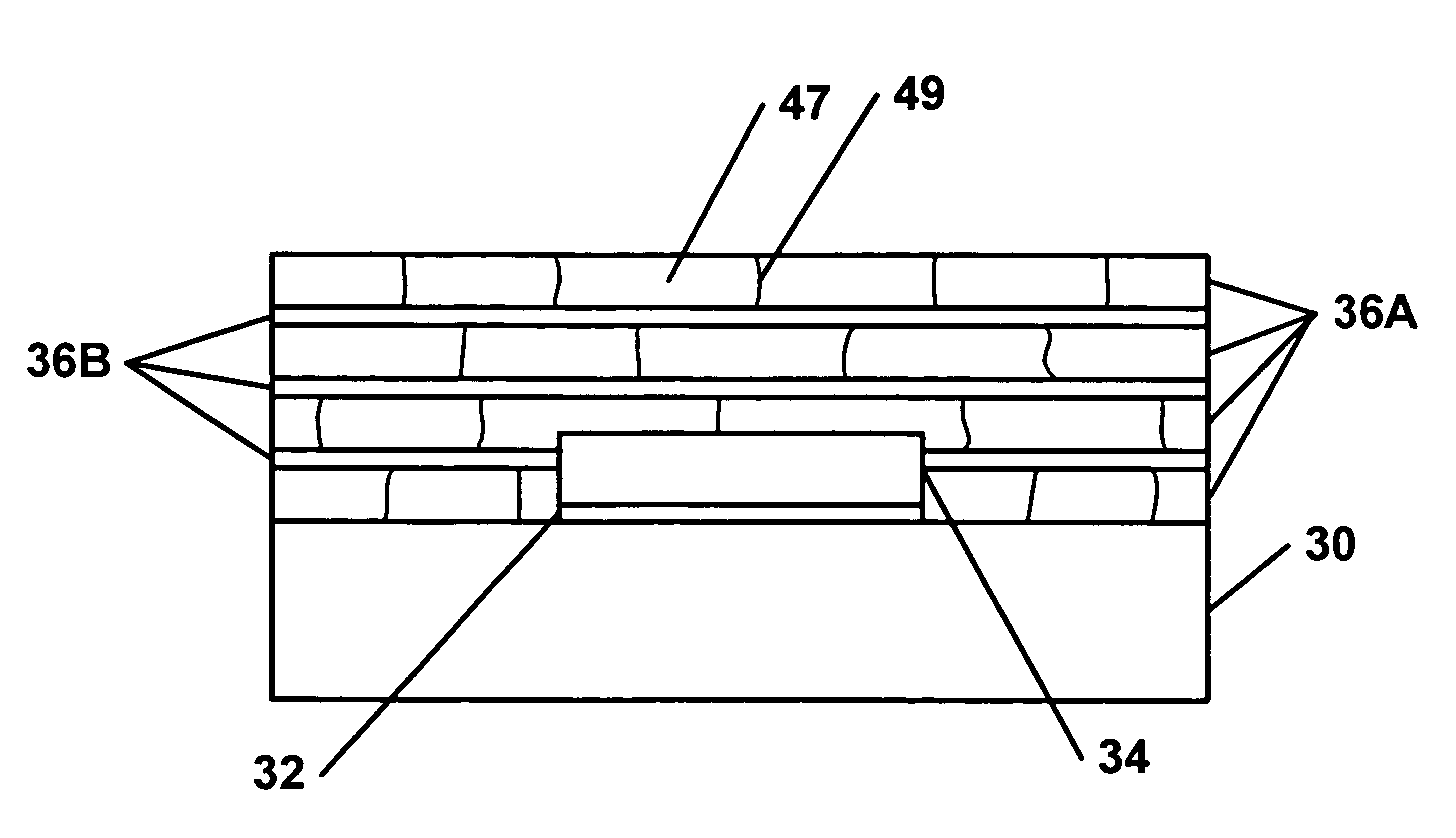
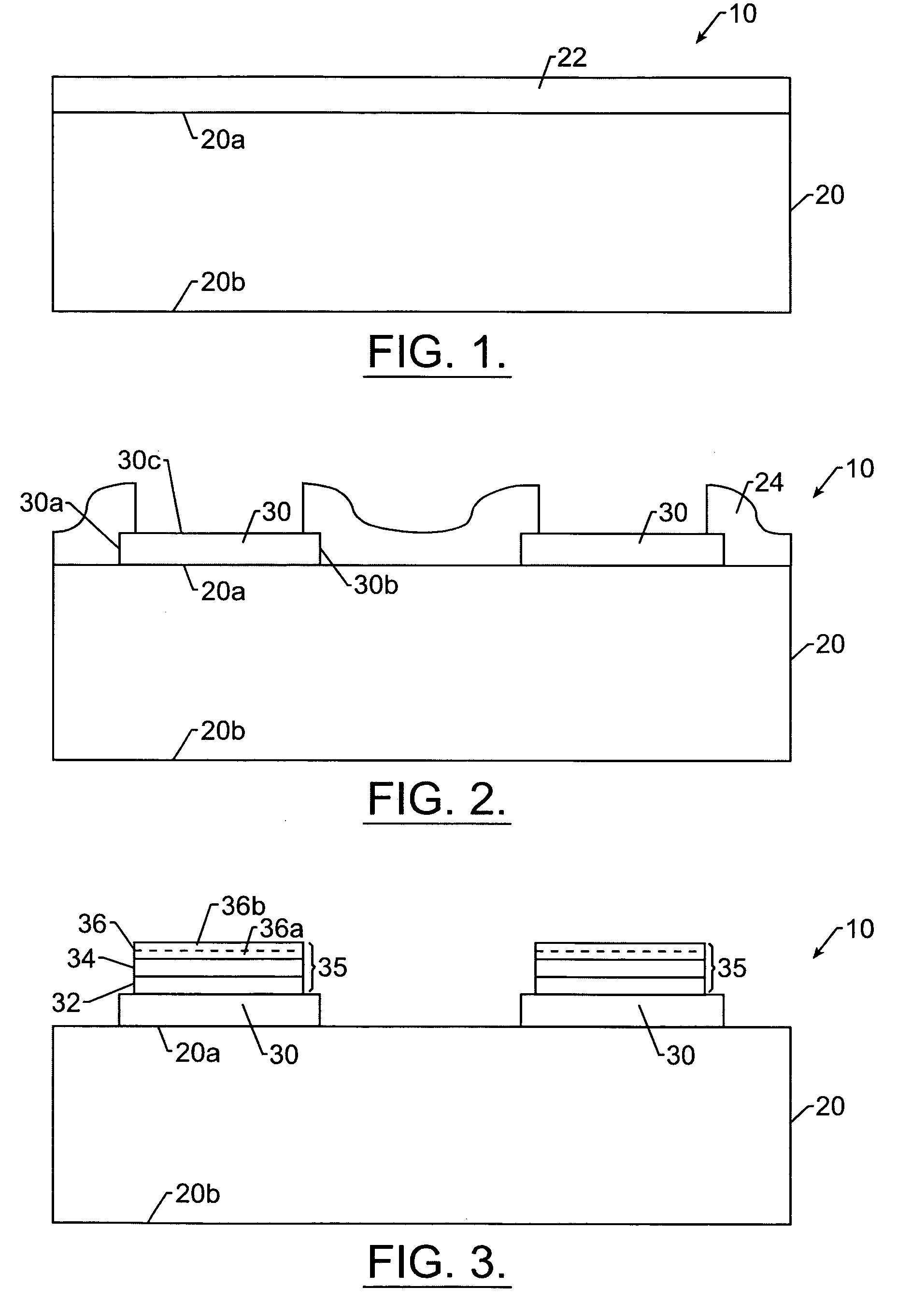
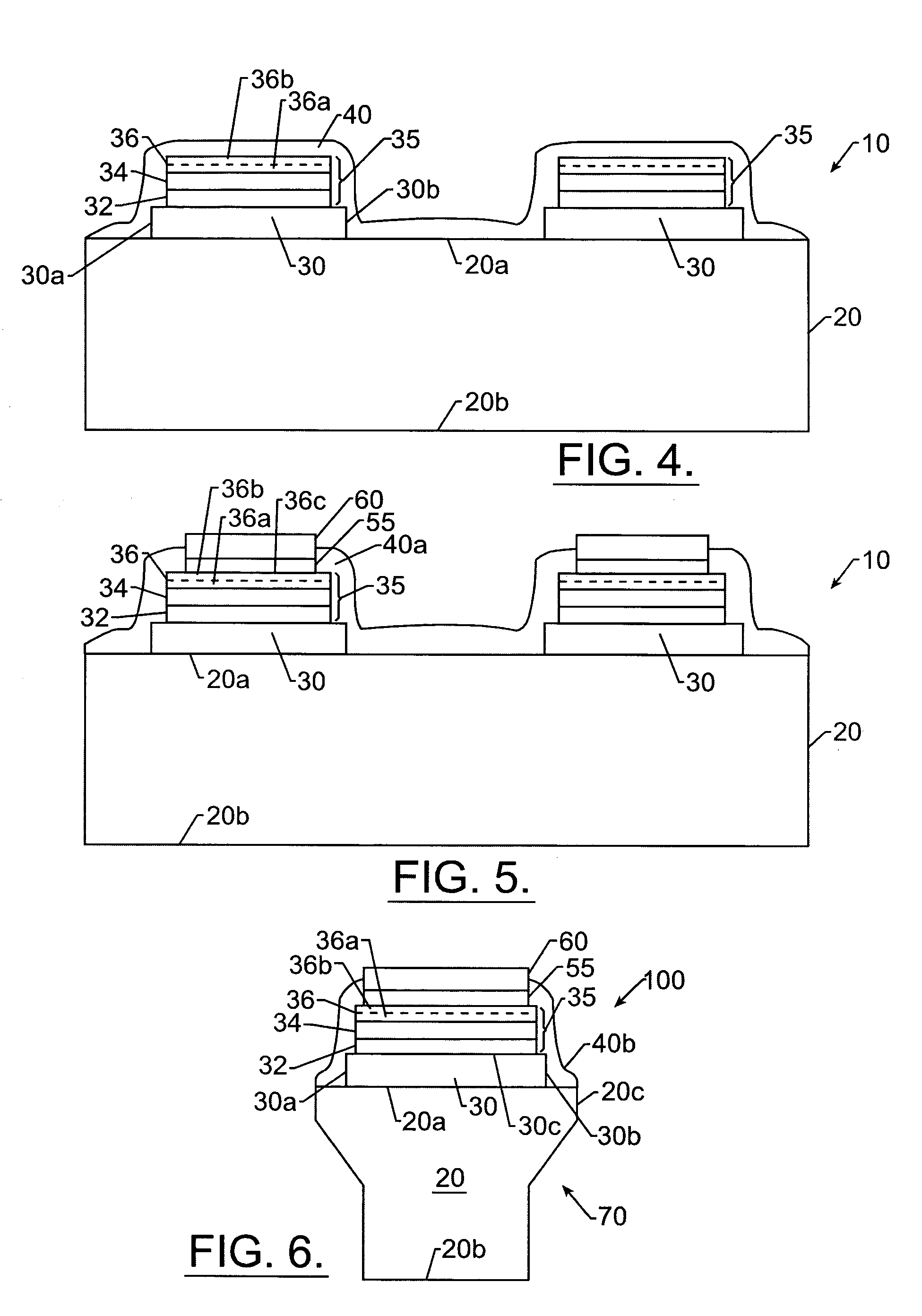
[0018]The present invention now will be described more fully hereinafter with reference to the accompanying figures, in which embodiments of the present invention are shown. This invention may, however, be embodied in many alternate forms and should not be construed as limited to the embodiments set forth herein.

[0019]Accordingly, while the present invention is susceptible to various modifications and alternative forms, specific embodiments thereof are shown by way of example in the drawings and will herein be described in detail. It should be understood, however, that there is no intent to limit the present invention to the particular forms disclosed, but on the contrary, the present invention is to cover all modifications, equivalents, and alternatives falling within the spirit and scope of the present invention as defined by the claims. Like numbers refer to like elements throughout the description of the figures. In the figures, the dimensions of layers and regions may be exagge...


PUM


Abstract

Semiconductor light emitting devices, such as light emitting diodes, include a substrate, an epitaxial region on the substrate that includes a light emitting region such as a light emitting diode region, and a multilayer conductive stack including a reflector layer, on the epitaxial region. A barrier layer is provided on the reflector layer and extending on a sidewall of the reflector layer. The multilayer conductive stack can also include an ohmic layer between the reflector and the epitaxial region. The barrier layer further extends on a sidewall of the ohmic layer. The barrier layer can also extend onto the epitaxial region outside the multilayer conductive stack. The barrier layer can be fabricated as a series of alternating first and second sublayers.

Description

CROSS-REFERENCE TO RELATED APPLICATIONS [0001]The present application is a continuation of PCT International Application No. PCT / US2003 / 021909, having an international filing date of Jul. 15, 2003. This application also claims the benefit of provisional Application Ser. No. 60 / 450,960, filed Feb. 28, 2003 to Slater et al., entitled Light Emitting Diodes Including Modifications for Submount Bonding and Manufacturing Methods Therefor, and is a continuation-in-part (CIP) of application Ser. No. 10 / 200,244, filed Jul. 22, 2002 now U.S. Pat. No. 6,740,906, to Slater et al., entitled Light Emitting Diodes Including Modifications for Submount Bonding and Manufacturing Methods Therefor, which itself claims the benefit of and priority from Provisional Application Ser. No. 60 / 352,941, filed Jan. 30, 2002, entitled LED Die Attach Methods and Resulting Structures, Provisional Application Ser. No. 60 / 307,311, filed Jul. 23, 2001, entitled Flip Chip Bonding of Light Emitting Diodes, and Provision...

Claims


Application Information

Patent Timeline
Patent Type & Authority Patents(United States)
IPC IPC(8): H01L33/00H01L33/20H01L33/40H01L33/44H01L33/62
CPCH01L33/405H01L33/44H01L33/32H01L33/60H01L33/20H01L33/62H01L2924/01057H01L2924/12041H01L2924/0002H01L2924/00
Inventor SLATER, JR., DAVID B.WILLIAMS, BRADLEY E.ANDREWSEDMOND, JOHN A.ALLEN, SCOTT T.
Owner CREELED INC
Why Eureka
Try Eureka