Memory gain cell

a memory gain and memory technology, applied in the field of memory cells, can solve the problems of increasing the power consumption of such memory, increasing the complexity of individual memory cells,

Active Publication Date: 2007-05-22
ANALOG DEVICES INC
View PDF11 Cites 30 Cited by
  • Summary
  • Abstract
  • Description
  • Claims
  • Application Information

AI Technical Summary

Benefits of technology

[0009]Accordingly, a memory cell, as contemplated herein, includes: a storage element (e.g., a capacitor however formed, including but not limited to a gate capacitance) on which a charge can be stored; a switch constructed and arranged to selectively connect the capacitor to a first data line, responsive to a first select signal; and a gain element having an input connected to receive a signal from the storage element and constructed and arranged to selectively transfer an output signal to a second data line, responsive to a second select signal. The switch can be a transistor such as a field-effect transistor, FET, having a first element (e.g., a drain) connected to the first data line, a second element (e.g., a source) connected to the storage element and a third, control element (e.g., a gate) connected to the first select signal. The gain element can be a tran

Problems solved by technology

Conventionally, adding access ports to a memory increases the complexity of the individual memory cells, for example i

Method used


Image

  • Memory gain cell
  • Memory gain cell
  • Memory gain cell

Examples


Embodiment Construction

[0018]This invention is not limited in its application to the details of construction and the arrangement of components set forth in the following description or illustrated in the drawings. The invention is capable of other embodiments and of being practiced or of being carried out in various ways. Also, the phraseology and terminology used herein is for the purpose of description and should not be regarded as limiting. The use of “including,”“comprising,” or “having,”“containing”, “involving”, and variations thereof herein, is meant to encompass the items listed thereafter and equivalents thereof as well as additional items.

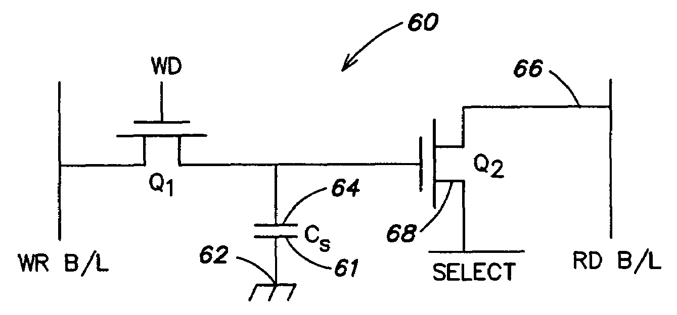
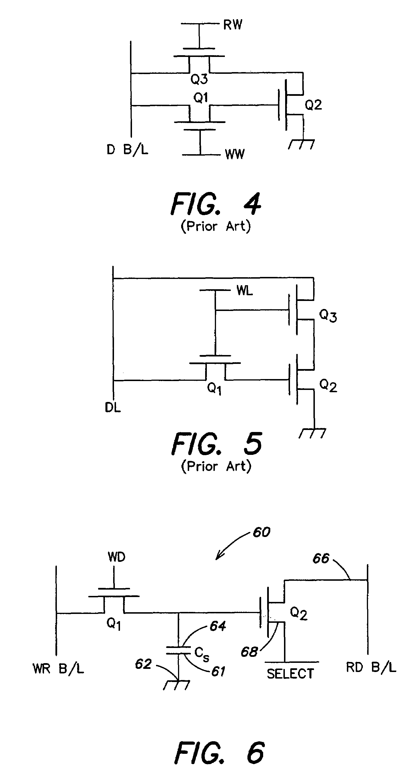
[0019]According to aspects of one embodiment of the invention, a memory cell includes only two transistors. The exemplary cell also is configured so that, when a collection of these cells is arranged in a regular array, the operations of writing data to cells and reading data from cells address the cells along orthogonal directions within the array. This allows...


PUM


Abstract

A memory cell includes: a charge storage element (e.g., capacitor); a switch constructed and arranged to selectively connect the charge storage element to a first data line, responsive to a first select signal; and a gain element having an input connected to receive a signal from the capacitor and constructed and arranged to selectively provide a corresponding output signal to a second data line, responsive to a second select signal. The switch can be a FET having a drain connected to the first data line, a source connected to the capacitor and a gate connected to the first select signal. The gain element can be a FET having a gate connected to the capacitor, a source connected to the second data line and a drain selectively connected to one of an upper power supply and a lower power supply. The switch can transfer a signal from the first data line onto the capacitor and can transfer a signal from the capacitor onto the first data line when selected by the first select signal. A two-dimensional array of such memory cells can be formed, wherein the first select signal and the second select signal orthogonally select cells, to facilitate matrix pivot operations and bit interleave/de-interleave operations. Also, a method of addressing an array of such memory cells can comprise: writing groups of bits linearly arrayed with respect to each other; and reading groups of bits linearly arrayed with respect to each other and orthogonally disposed to the groups of bits written.

Description

FIELD OF THE INVENTION[0001]The present invention relates to memory cells. Somewhat more particularly, the invention relates to those memory cells known as gain cells and to memory configurations using gain cells.BACKGROUND OF INVENTION[0002]Numerous memory cell configurations are known in the art. Each possesses advantages and disadvantages, some advantages and disadvantages being related to the number of transistors employed. Skilled artisans frequently classify the various configurations into groups according to the number of transistors associated with a single storage element present in a single memory cell. Thus a circuit including a storage element coupled to but a single transistor is referred to as a 1T cell, as illustrated schematically in FIG. 1. The cell has simply a storage element, CS, and a single transistor, Q1, that functions as a transfer gate element. Applying the same taxonomy, a cell including a single storage element coupled to three transistors is referred to ...

Claims


Application Information

Patent Timeline
IPC IPC(8): G11C11/24G11C11/405G11C11/406
CPCG11C11/405
Inventor PENCHUK, ROBERT A.
Owner ANALOG DEVICES INC
Why Eureka
Try Eureka