

Method and apparatus for 3D interconnect
a technology of 3d interconnection and abrasive layer, which is applied in the direction of printed circuit manufacturing, printed circuit aspects, conductive pattern formation, etc., can solve the problems of time-consuming and expensive polishing to remove such a large range of overburden depths, and implement a cost- and time-efficient integrated circuit fabrication system. , to achieve the effect of good adhesion
- Summary
- Abstract
- Description
- Claims
- Application Information
AI Technical Summary
Benefits of technology
Problems solved by technology
Method used
Image

Examples
Embodiment Construction
[0001]1. Field of the Invention
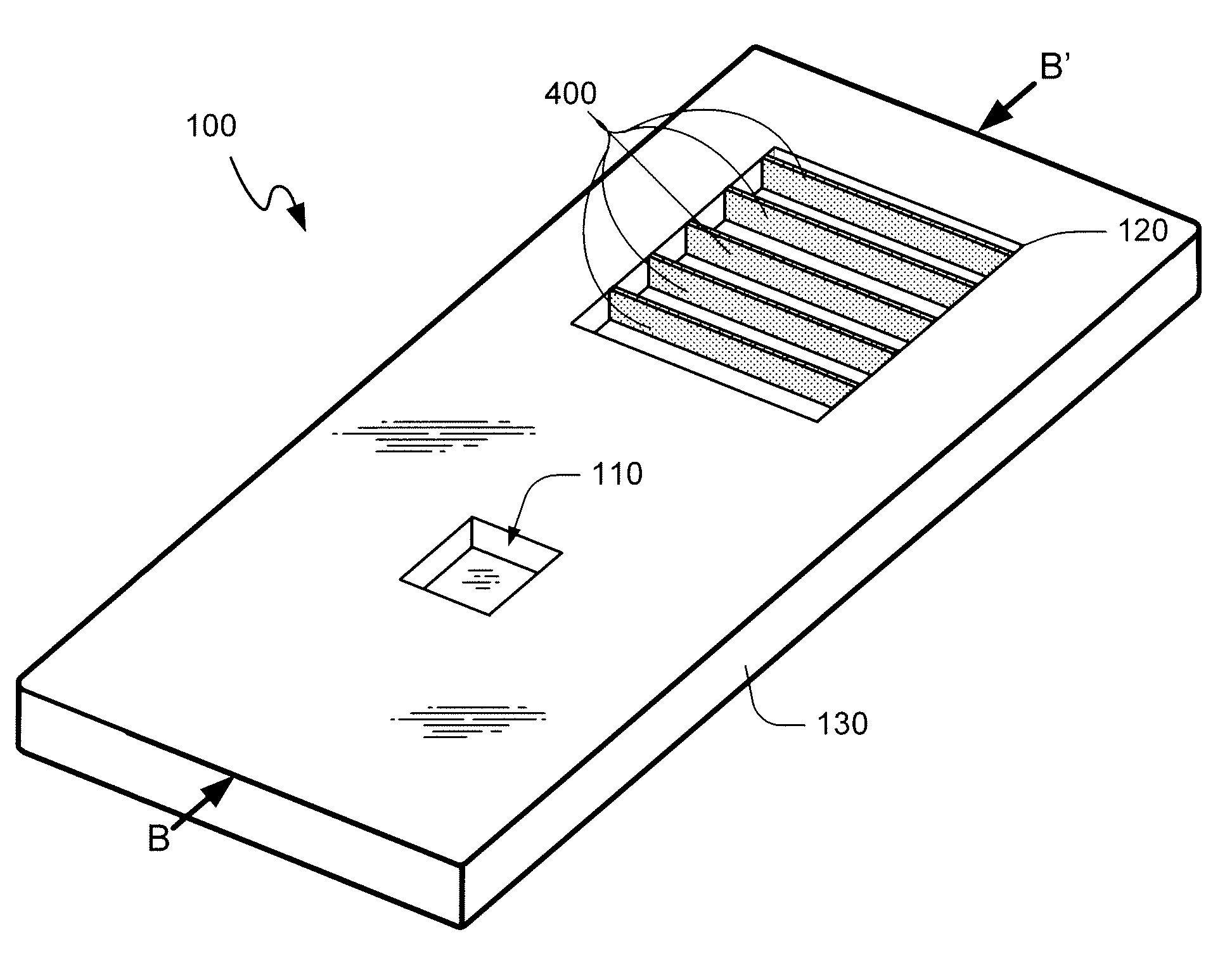
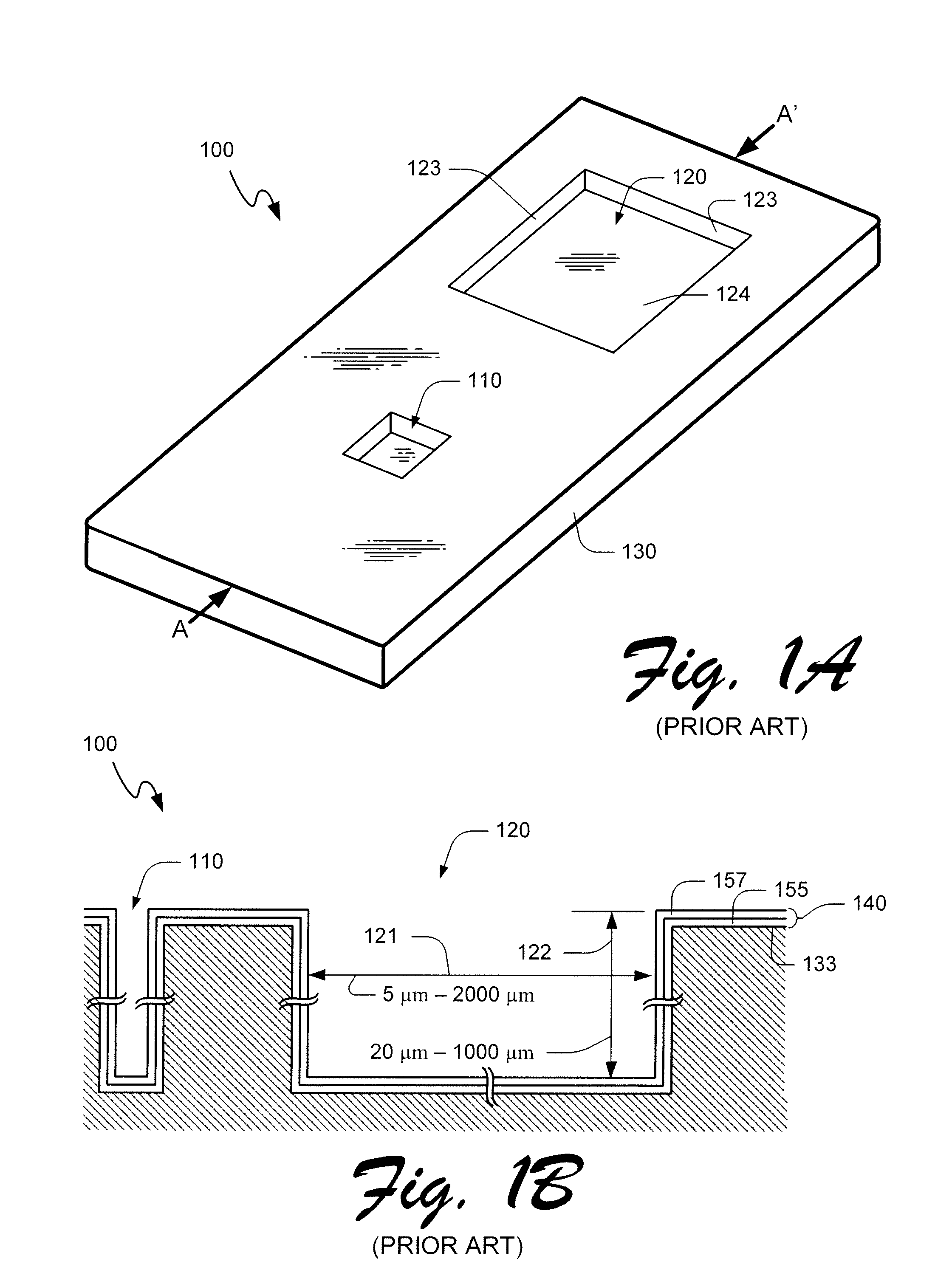
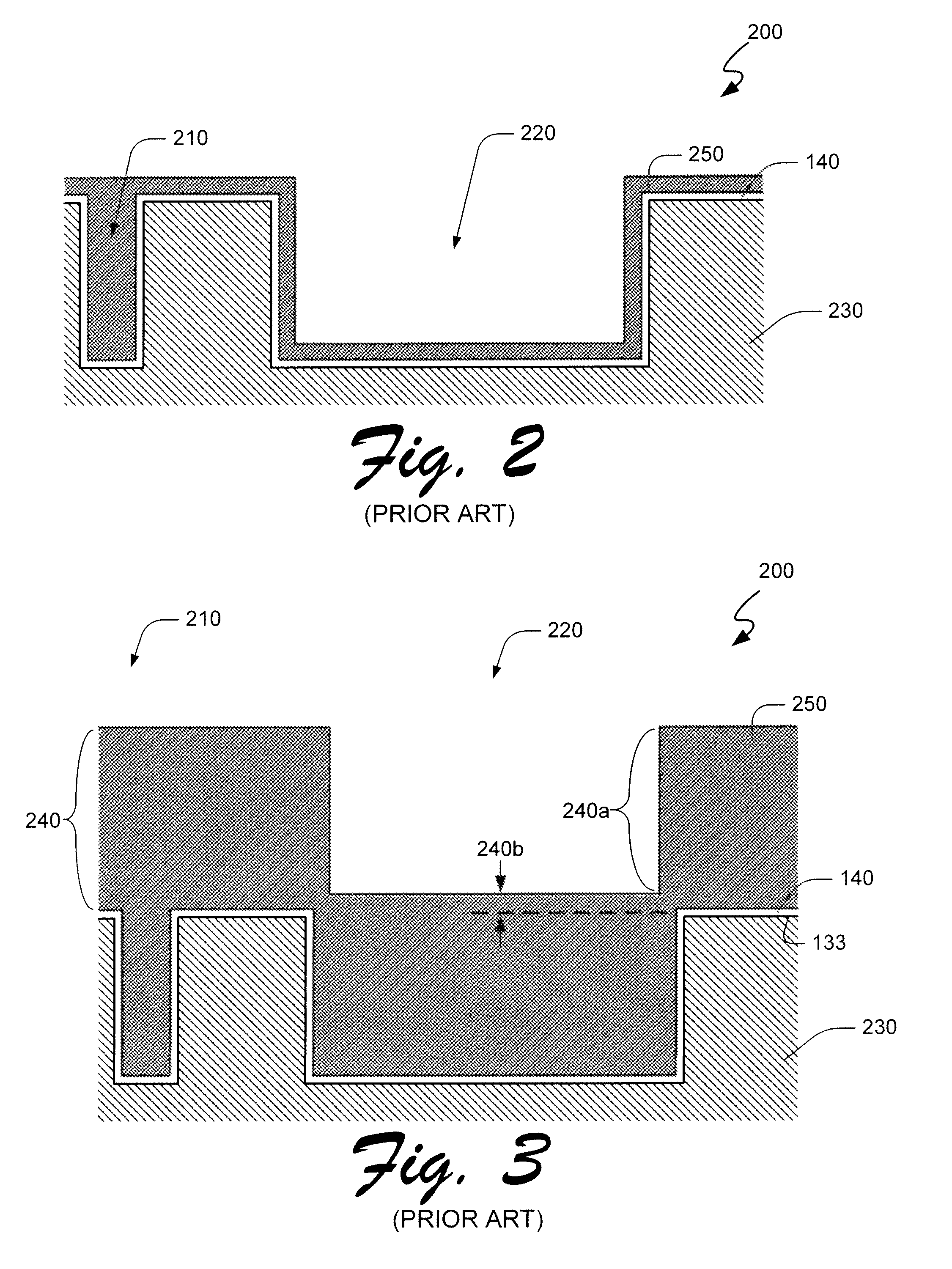
[0002]The present invention relates to a method and apparatus for providing electrical interconnects. More specifically, the present invention relates to fabricating connective structures within defined areas of a substrate such as a semiconductor wafer, a semiconductor chip, a multichip module, or a printed wiring assembly. Further, the present invention relates to embodiments of electrically reactive interconnect components.
[0003]2. Background of the Invention
[0004]Creating electrical interconnections is a challenging and essential part of manufacturing compact electronic components and systems, particularly in the field of manufacturing integrated circuits. Over time, automated methods have been developed to deposit conductive materials on substrates, in layers of substrates, or through cavities such as trenches, holes, and vias of a substrate. Deposition of materials in such cavities provides for electrical interconnections between conductive trace...
PUM
| Property | Measurement | Unit |
|---|---|---|
| thickness | aaaaa | aaaaa |
| diameter | aaaaa | aaaaa |
| depth | aaaaa | aaaaa |
Abstract
Description
Claims
Application Information