Light-emitting apparatus and production method thereof

a technology of light-emitting apparatus and production method, which is applied in the direction of semiconductor devices, solid-state devices, transistors, etc., can solve the problems of high cost, increased production cost, and increased production cost, so as to reduce the aperture ratio of the device, the effect of suppressing the degradation of the organic layer

Active Publication Date: 2010-04-08
CANON KK
View PDF25 Cites 409 Cited by
  • Summary
  • Abstract
  • Description
  • Claims
  • Application Information

AI Technical Summary

Benefits of technology

[0028]An object of the present invention is to form a display apparatus or the like which has an OS-TFT as a field effect transistor for driving an organic EL device (typ

Problems solved by technology

However, the amorphous Si semiconductor and the organic semiconductor each have a low mobility.
In addition, the polycrystalline Si semiconductor is difficult to increase the area thereof and necessitates a high cost.
Further, the polycrystalline Si semiconductor has grain boundaries, and the characteristics of a device formed thereof will vary owing to carrier scattering, so that a circuit for suppressing the luminance unevenness of the device is separately required to be provided, and the requirement is responsible for an additional increase in the production cost and a reduction in the aperture ratio of the device.
The reason for this is that a dehydration time of less than 10 minutes results in an insufficient dehydration treatment, so that it may be difficult to reduce the water content of an organic light-emitting medium after the assembly to 0.05 wt % or less, and further that a dehydration time in excess of 12 hours merely lengthens the time period for the heat treatment and the effect exerted by more than 12 hours of heat treatment may be not different from that exerted by 12 hours or less of heat treatment.
However, the water vapor barrier property of an insulating film tends to be reduced owing to the film formation at the lower temperature, with the result that a sufficient effect is hardly obtained.
The reason is considered that when film formation is performed by a low temperature process (for example, 300° C. or less), it becomes difficult to form a dense film.
On the other hand, an oxide generally has higher polarization property than that of amorphous Si or polycrystalline Si, so that there is a tendency for the oxide to be extremely liable to adsorb moisture.
Becaus

Method used


Image

  • Light-emitting apparatus and production method thereof
  • Light-emitting apparatus and production method thereof
  • Light-emitting apparatus and production method thereof

Examples


embodiment 1

[0050]In this embodiment, a description is made of a case where OS-TFTs of an amorphous In—Ga—Zn—O system are used as switching devices, and an organic EL display panel according to a typical constitution of the present invention, that is, a constitution in which organic EL devices are stacked on the same substrate as the substrate on which the OS-TFTs are formed is produced. The term “In—Ga—Zn—O system” herein employed refers to an oxide-based material containing at least In, Ga, and Zn.

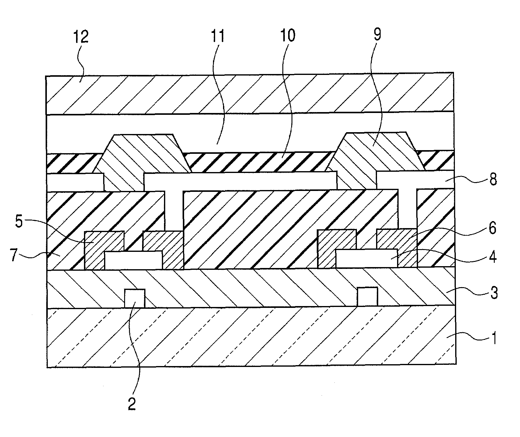
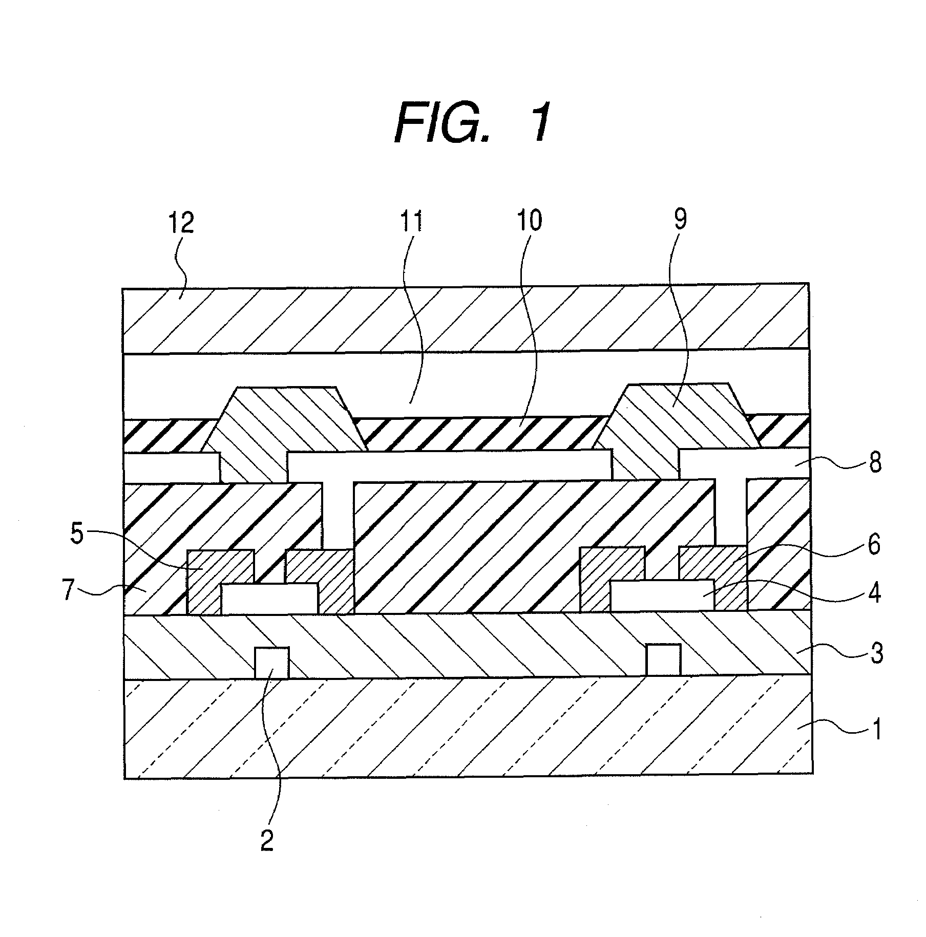
[0051]FIG. 1 is a cross-sectional view illustrating the constitution of a light-emitting apparatus as an embodiment of the present invention.

[0052]In FIG. 1, reference numeral 1 denotes a glass substrate as a substrate; 2, a gate electrode; 3, a gate insulating layer; 4, an oxide semiconductor layer (semiconductor layer); 5, a drain electrode; 6, a source electrode; 7, an insulating layer; 8, a transparent anode as a lower electrode; 9, a device separation film that can be provided as needed; 10, an...

example

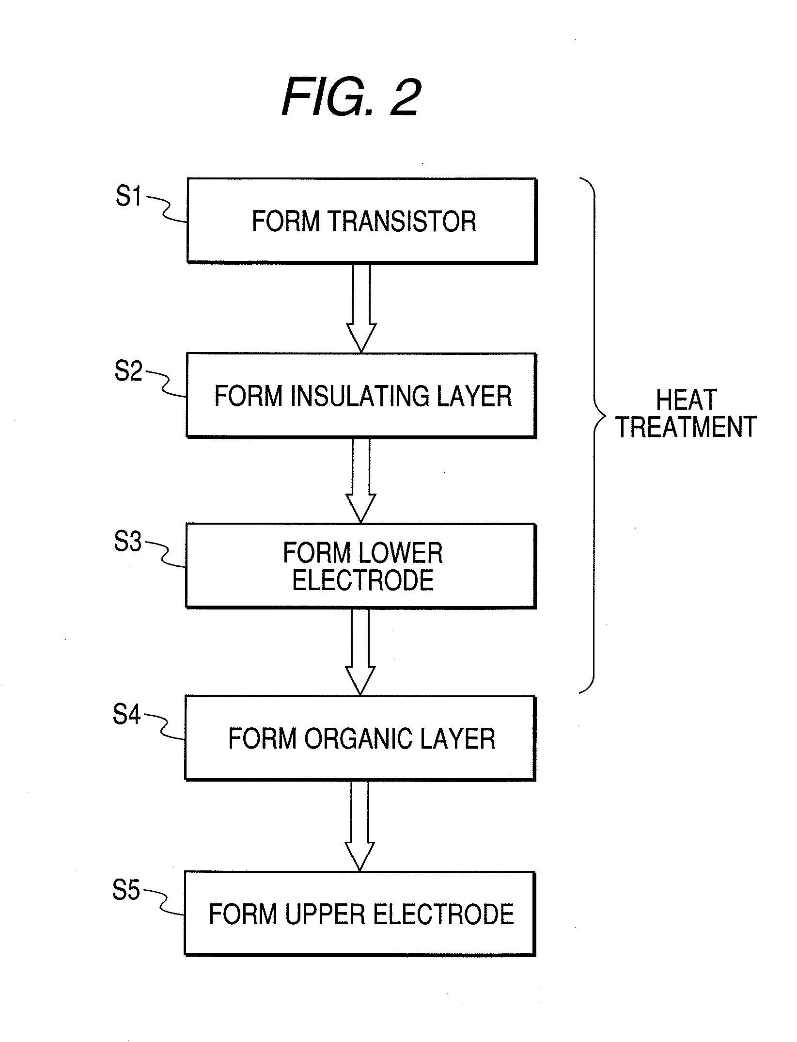
[0128]Hereinafter, an example of a production method in which organic EL devices and OS-TFTs are mounted on the same substrate will be described with reference to FIG. 5. The maximum temperature which can be reached during a process for the formation of the organic EL device is 150° C.

[0129]In addition, in order that the device may be prevented from unnecessarily adsorbing moisture owing to exposure to the atmosphere, the device is kept so as not to be brought into contact with the atmosphere by appropriately using, for example, a transfer vessel except during a process utilizing a photolithographic method and a wet process.

(Formation of Field Effect Transistor)

[0130]A glass substrate 1 (1737 (trade name); manufactured by Corning Inc.) is selected as a substrate on which a film is to be formed. Before the formation of a film, the substrate is ultrasonically degreased and cleaned sequentially with acetone, IPA, and ultrapure water for 5 minutes each, and is then subjected to a heat t...


PUM

PropertyMeasurementUnit
Temperatureaaaaaaaaaa
Semiconductor propertiesaaaaaaaaaa

Abstract

Provided is a method of producing a light-emitting apparatus having a field effect transistor for driving an organic EL device, the field effect transistor including an oxide semiconductor containing at least one element selected from In and Zn, the method including the steps of: forming a field effect transistor on a substrate; forming an insulating layer; forming a lower electrode on the insulating layer; forming an organic layer for constituting an organic EL device on the lower electrode; forming an upper electrode on the organic layer; and after the step of forming the semiconductor layer of the field effect transistor and before the step of forming the organic layer, performing heat treatment such that an amount of a component that is desorbable as H2O from the field effect transistor during the step of forming the organic layer is less than 10−5 g/m2.

Description

TECHNICAL FIELD[0001]The present invention relates to a light-emitting apparatus and a method of producing the apparatus, in particular, a light-emitting apparatus using a field effect transistor as a switching device and typically obtained by stacking an organic EL device on the same substrate as the substrate on which the transistor is formed, and a method of producing the apparatus.BACKGROUND ART[0002]The so-called active matrix system in which field effect transistors formed on a substrate are used has been adopted as one system according to which an organic EL panel is driven.[0003]In this system, because the luminance of an organic EL device is controlled with a current, a field effect transistor the mobility of which is so large that a sufficient current can be flowed therein is suitably used.[0004]At present, for example, an amorphous Si semiconductor, a polycrystalline Si semiconductor, or an organic semiconductor has been used in a field effect transistor. However, the amo...

Claims


Application Information

Patent Timeline
IPC IPC(8): H01L29/786H01L21/30H01L33/00
CPCH01L51/0037H01L29/66969H01L27/1214H01L29/78606H01L29/7869H01L27/3262H01L29/66742H01L51/0026H01L51/5237H01L27/127H01L27/1225H10K59/1213H10K71/40H10K85/1135H10K59/87H10K50/84
Inventor WATANABE, TOMOHIRO
Owner CANON KK
Why Eureka
Try Eureka