Composite comprised of flat conductor elements

a technology of conductor elements and composites, which is applied in the direction of printed circuit parts, sustainable manufacturing/processing, final product manufacturing, etc., can solve the problems of inability to use the entire composite, inability to arbitrarily reduce the distance between the solder pads, and too little solder material on the actual contact face, etc., to achieve sufficient protection against air bridges, reduce the distance between the strip conductors, and ensure the quality of solder connections

Inactive Publication Date: 2007-05-29
DR JOHANNES HEIDENHAIN GMBH
View PDF24 Cites 8 Cited by
  • Summary
  • Abstract
  • Description
  • Claims
  • Application Information

AI Technical Summary

Benefits of technology

[0011]Therefore an object of the present invention is based on providing a composite of flat elements supporting strip conductors, wherein the amount of the distance between the strip conductors can be minimized. Further than that it is intended to achieve sufficient protection against air bridges, even with short distances between the individual strip conductors, and to assure the good quality of the soldered connections.

Problems solved by technology

If now, because of process-related fluctuations, the volume of the applied solder is too large, the excess solder will exit the area of the solder pads, which can lead to the formation of short circuits between the strip conductors, so that the entire composite becomes unusable.
Therefore the distances between the solder pads cannot be arbitrarily reduced.
In this case there is a tendency of too little solder material being available on the actual contact face.

Method used


Image

  • Composite comprised of flat conductor elements
  • Composite comprised of flat conductor elements
  • Composite comprised of flat conductor elements

Examples


Embodiment Construction

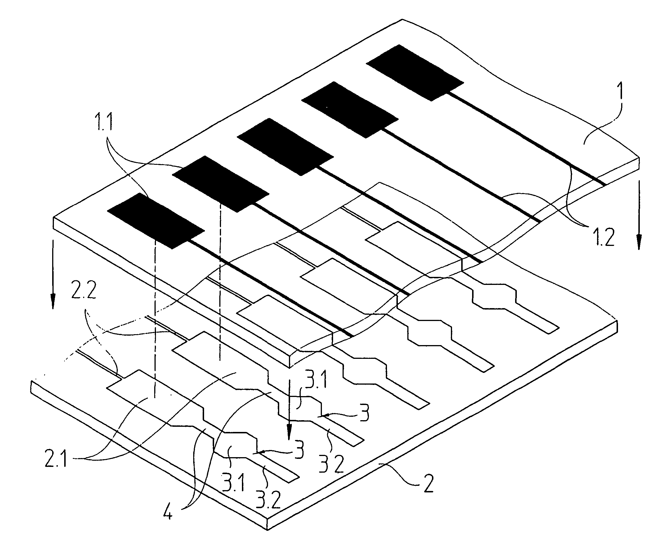
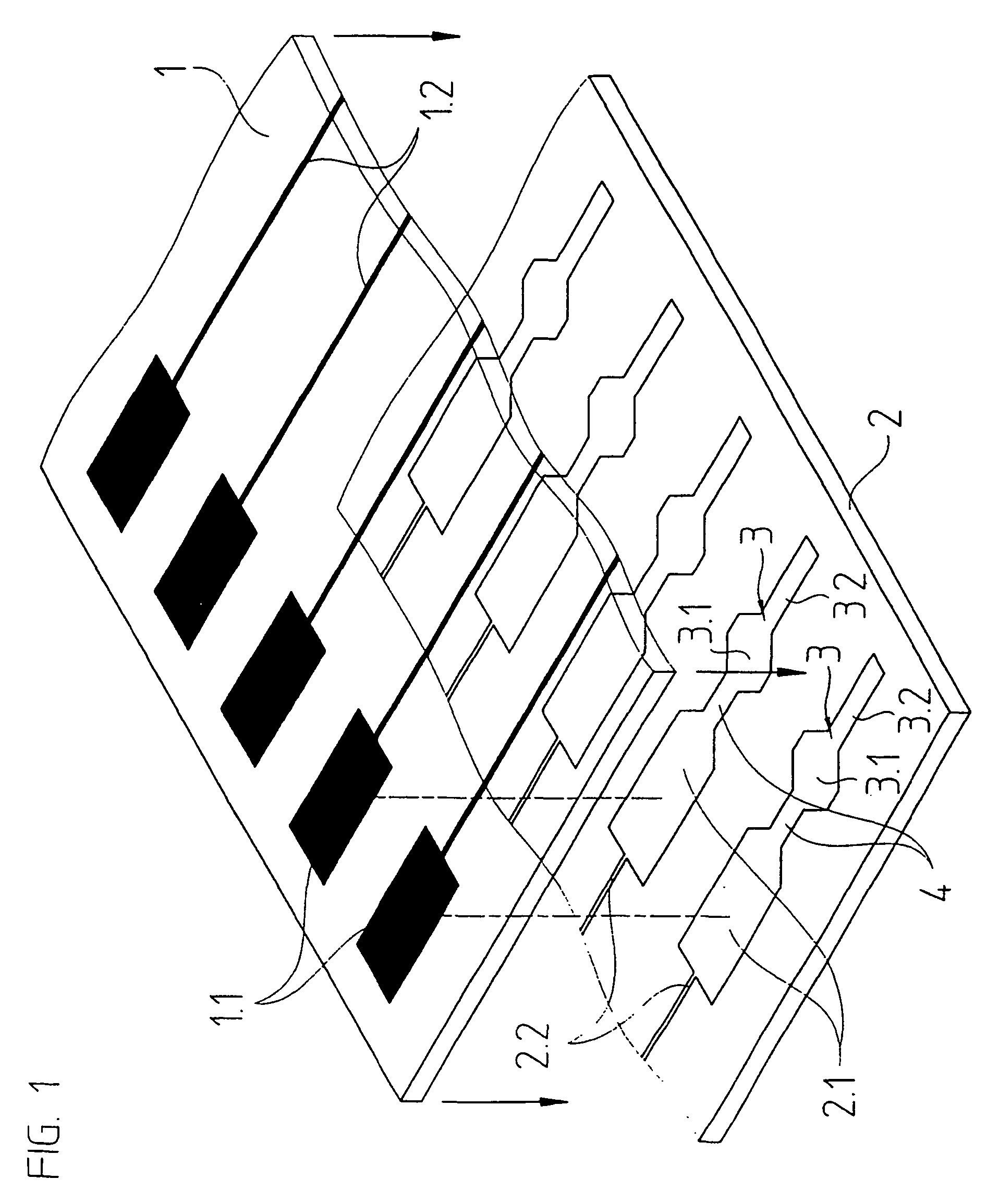
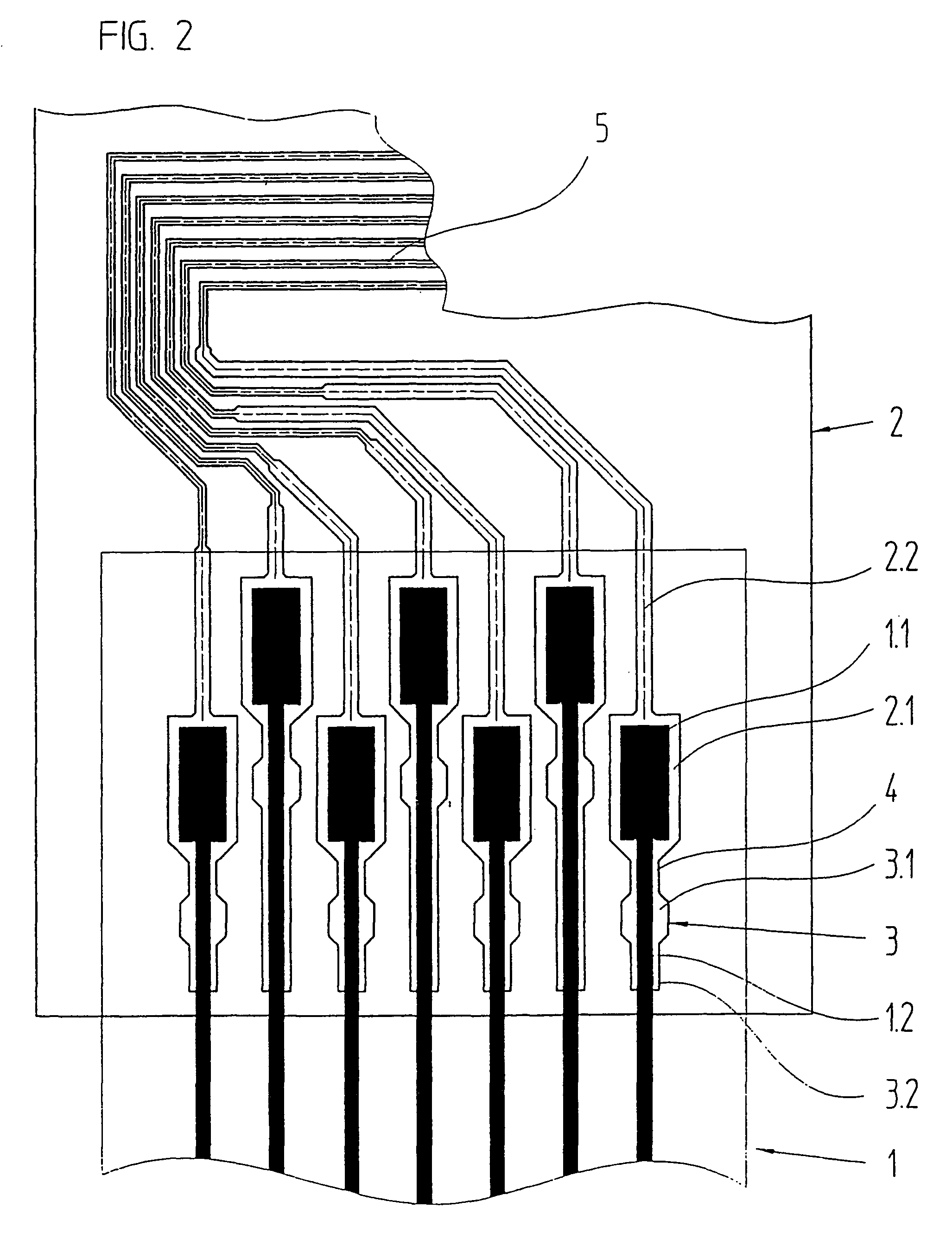
[0022]A spatial representation of a composite is shown in FIG. 1 which, for the sake of clarity, is embodied in an exploded view. Solder pads 1.1 including a 15 μm to 20 μm thick copper layer are attached to the underside of an approximately 50 μm thick flexible strip conductor foil 1 made of polyimide. Moreover, strip conductors 1.2, also made of copper and having approximately the same layer thickness as the solder pads 1.1, are also located on this side of the strip conductor foil 1. Electrical signals are transmitted via the strip conductors 1.2 to an electronic element, not further represented.

[0023]A printed circuit board 2 made of glass is arranged opposite the strip conductor foil 1. Solder pads 2.1, strip conductors 2.2, solder shunting areas 3 and link areas 4 of copper of a layer thickness of approximately 3 μm are applied to the printed circuit board 2. If required, a coupling agent is provided on the printed circuit board 2 prior to applying the copper layer. The link a...


PUM

PropertyMeasurementUnit
thickaaaaaaaaaa
thickaaaaaaaaaa
thickaaaaaaaaaa

Abstract

A composite of at least two flat elements that includes a first support substrate having a first solder pad, and a second support substrate having a second solder pad that is soldered together with the first solder pad. Strip conductor structures are applied to the first support substrate and the second support substrate and a link area that connects a solder shunting area with the first solder pad, wherein the link area is narrower than the first solder pad and the solder shunting area.

Description

[0001]Applicants claim, under 35 U.S.C. §§ 120 and 365, the benefit of priority of the filing date of Feb. 14, 2002 of a Patent Cooperation Treaty patent application, copy attached, Ser. No. PCT / EP02 / 01590, filed on the aforementioned date, the entire contents of which are incorporated herein by reference, wherein Patent Cooperation Treaty patent application Ser. No. PCT / EP02 / 01590 was not published under PCT Article 21(2) in English.[0002]Applicants claim, under 35 U.S.C. § 119, the benefit of priority of the filing date of Mar. 9, 2001 of a German patent application, copy attached, Ser. No. 101 11 389.7, filed on the aforementioned date, the entire contents of each of which are incorporated herein by reference.BACKGROUND OF THE INVENTION[0003]1. Field of the Invention[0004]The present invention relates to a composite of flat conducter elements having solder shunting areas. The present invention also relates to the use of this composite in sensor elements.[0005]2. Description of th...

Claims


Application Information

Patent Timeline
Patent Type & Authority Patents(United States)
IPC IPC(8): H05K1/00H05K1/11H05K3/34H05K1/14H05K3/36
CPCH05K1/111H05K3/363H05K2201/09709H05K2201/09727H05K2201/09781H05K2203/046H01L2924/00013H01L2224/29099Y02P70/50
Inventor RISSING, LUTZFISCHER, PETER
Owner DR JOHANNES HEIDENHAIN GMBH
Why Eureka
Try Eureka