Precasting multi-layer PCB process

a pcb and multi-layer technology, applied in printed circuit assembling, resistive material coating, foundry moulds, etc., can solve the problems of circuitry being vulnerable to shortage or interruption, huge consumption of materials and process facilities, and high production costs, so as to improve the quality of pcb and improve the mechanical strength

Inactive Publication Date: 2007-06-05
YANG HO CHING
View PDF5 Cites 4 Cited by
  • Summary
  • Abstract
  • Description
  • Claims
  • Application Information

AI Technical Summary

Benefits of technology

[0009]The primary purpose of the present invention is to provide a pre-casting process for the manufacturing of multi-layer PCB to correct the flaws found with the prior art and to upgrade the quality of the PCB. To achieve the purpose, a fiberglass substrate is drilled and stuffed with a conductive material. A steel mold engraved with circuitry is coated with epoxy. Both of the mold and the substrate are bound to each other and then the epoxy is fixed to the substrate after the mold is removed. The epoxy is coated with a conductive material for the latter to be consistently distributed on the circuitry of epoxy, air bulb vacuum removed, baked, sandblasted to remove the film, and rinsed before inserting the conductive material in the epoxy circuitry to come up the finished product of the PCB. Finally, upon the lamination of multiple layers, the circuitry on the most outer layer where pending soldering is plated to improve its mechanical strength.

Problems solved by technology

The manufacturing process of the prior art is found with the following flaws:1. Complicated, consuming too much efforts and time, thus resulting in higher production cost;2. In the process of lamination, stress from high pressure usually winds up deformed PCB and variations in dimension; and3. Enormous consumption of materials and size of process facilities to prevent easier production scheduling.
Otherwise, the circuitry is vulnerable to shortage or interruption, and insufficient strength.

Method used


Image

  • Precasting multi-layer PCB process
  • Precasting multi-layer PCB process
  • Precasting multi-layer PCB process

Examples


Embodiment Construction

[0020]The following descriptions are of exemplary embodiments only, and are not intended to limit the scope, applicability or configuration of the invention in any way. Rather, the following description provides a convenient illustration for implementing exemplary embodiments of the invention. Various changes to the described embodiments may be made in the function and arrangement of the elements described without departing from the scope of the invention as set forth in the appended claims.

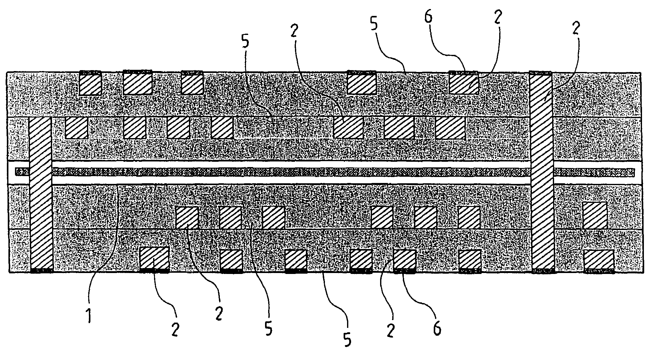
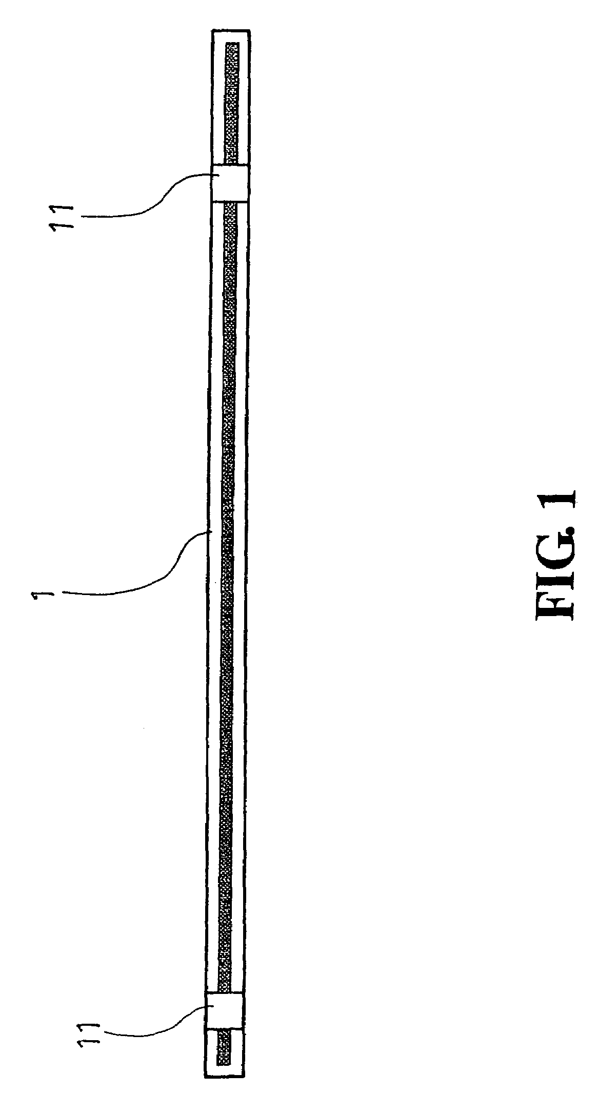
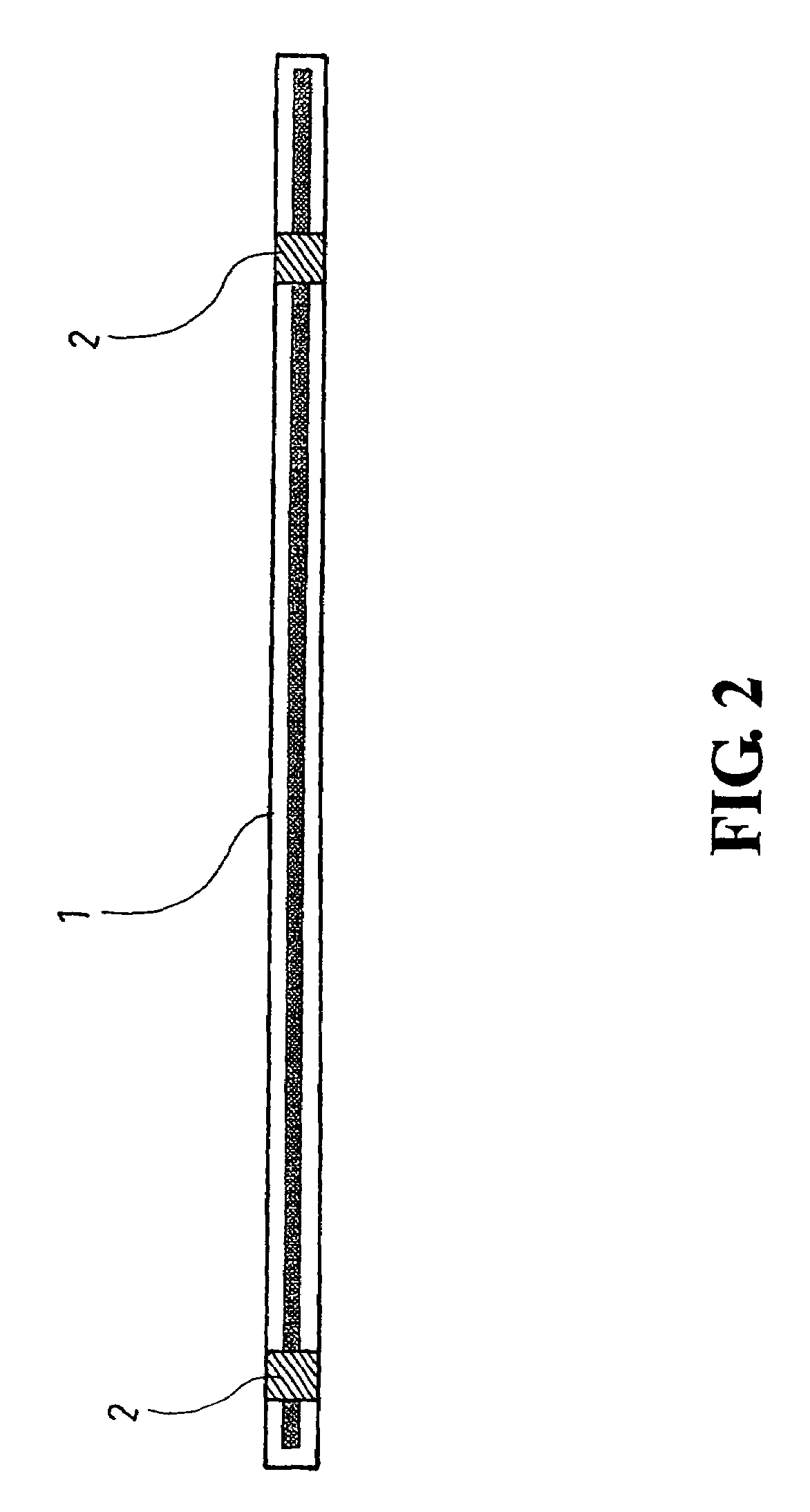
[0021]Referring to FIGS. 1 through 7, the multi-layer PCB manufacturing process of the present invention is essentially comprised of the following steps:[0022]1. Multiple through holes 11 are drilled through the fiberglass substrate 1 as illustrated in FIG. 1.[0023]2. Each through hole 11 on the substrate 1 is stuffed with a conductive material 2 as illustrated in FIG. 2.[0024]3. An upper and a lower steel molds 3, 4 are provided and engraved with floated circuitries 31, 41 (the printed circuitry...


PUM

PropertyMeasurementUnit
conductiveaaaaaaaaaa
mechanical strengthaaaaaaaaaa
structural strengthaaaaaaaaaa

Abstract

A pre-casting multi-layer PCB process has steel plate mold engraved with circuitry and the epoxy coated on the mold for the epoxy to cover up a fiber glass substrate; conductive material coated on the epoxy to insert molding the former into the latter to form recessed circuitry; then baked and solidified, sandblasted to remove film for the conductive material to become conducted circuitry; the lamination made by layer for achieving even thinner PBC circuitry while maintaining sufficient structural strength.

Description

BACKGROUND OF THE INVENTION[0001](a) Technical Field of the Invention[0002]The present invention is related to a pre-casting multi-layer PCB process, and more particularly, to one that allows even thinner circuitry, higher structural strength, lower production cost, and easier production planning.[0003](b) Description of the Prior Art[0004]In the manufacturing process for the single layer or multi-layer PCB of the prior art, a negative is needed to be exposed for image transfer of the circuitry on a substrate with a copper foil surface, then etched, drilled, and plated; while in case of multi-layer PCB, additional process of high pressure lamination is required. The manufacturing process of the prior art is found with the following flaws:[0005]1. Complicated, consuming too much efforts and time, thus resulting in higher production cost;[0006]2. In the process of lamination, stress from high pressure usually winds up deformed PCB and variations in dimension; and[0007]3. Enormous cons...

Claims


Application Information

Patent Timeline
Patent Type & Authority Patents(United States)
IPC IPC(8): H05K3/20
CPCH05K3/4614H05K3/465H05K3/0014Y10T29/49158H05K3/107H05K2201/09036H05K2201/10378H05K2203/025H05K2203/061H05K2203/063Y10T29/49155Y10T29/49126Y10T29/49165Y10T29/49128H05K3/045
Inventor YANG, HO-CHING
Owner YANG HO CHING
Why Eureka
Try Eureka