Semiconductor device including ladder-shaped siloxane hydride and method for manufacturing same

a technology of siloxane hydride and semiconductor devices, which is applied in the direction of basic electric elements, chemical vapor deposition coatings, coatings, etc., can solve the problems of insufficient mechanical performance and/or plasma resistance of films having lower dielectric constants, insufficient adhesiveness, and insufficient adhesion between films, etc., to achieve the effect of effectively inhibiting the introduction of moisture, improving the reliability of semiconductor devices, and improving the integration level of semiconductor devices

Active Publication Date: 2007-06-12
RENESAS ELECTRONICS CORP
View PDF33 Cites 9 Cited by
  • Summary
  • Abstract
  • Description
  • Claims
  • Application Information

AI Technical Summary

Benefits of technology

[0015]In view of the above situation, the present invention provides a solution to the above-mentioned problems, and it is an object of the present invention to reduce the effective dielectric constant of the insulating film while maintaining better reliability of the semiconductor device, which otherwise may be deteriorated by a moisture absorption.
[0022]According to yet other aspect of the present invention, the semiconductor device may further comprise a metal interconnect embedded in a multilayer structure, the multilayer structure comprising the first insulating film and the second insulating film. According to further aspect of the present invention, the above-mentioned method for manufacturing the semiconductor device may further comprise: after forming the second insulating film, selectively removing the second insulating film and the first insulating film to form an interconnect groove; and filling the interconnect groove with a metal to form a metal interconnect. Further, semiconductor devices such as transistors may be formed on the semiconductor substrate. Since the interlayer insulating film having the ladder-shaped siloxane hydride according to the present invention can effectively inhibit the introduction of moisture, it is possible to have a configuration of free of a guard ring. That is, it is possible to improve the reliability of the semiconductor device while maintaining higher integration level of the semiconductor device.

Problems solved by technology

The films having lower dielectric constant generally have insufficient mechanical performances and / or plasma resistance.
However, the above layer constitution may cause insufficient adhesiveness between the insulating film having lower dielectric constant and the protective film.
Since the MSQ film 2 comprises an organic material and the silicon oxide film 4 comprises an inorganic material, the insufficient adhesion may occur between these films, and further the peeling off therebetween may be caused in the extreme cases.
First, the layer constitution shown in FIG. 1 may have a problem, in which it is easier to introduce moisture within the devices having such layer constitution.
This configuration may also cause the increase of the dielectric constant of the interlayer insulating film.
The introduction of moisture into the semiconductor device may cause an erosion of the metal interconnects or degrade the performances of the device by the uptake of moisture, thereby considerably deteriorating the reliability of the device.
However, the configuration of providing the guard ring has reduced areas, on which devices are formed, and therefore the presence of the guard ring may be a factor of inhibiting the higher integration.

Method used


Image

  • Semiconductor device including ladder-shaped siloxane hydride and method for manufacturing same
  • Semiconductor device including ladder-shaped siloxane hydride and method for manufacturing same
  • Semiconductor device including ladder-shaped siloxane hydride and method for manufacturing same

Examples


first embodiment

[0059]FIGS. 9A to 9D are the cross sectional views showing the processing steps of the process for forming the semiconductor device according to the first preferred embodiment of the present invention.

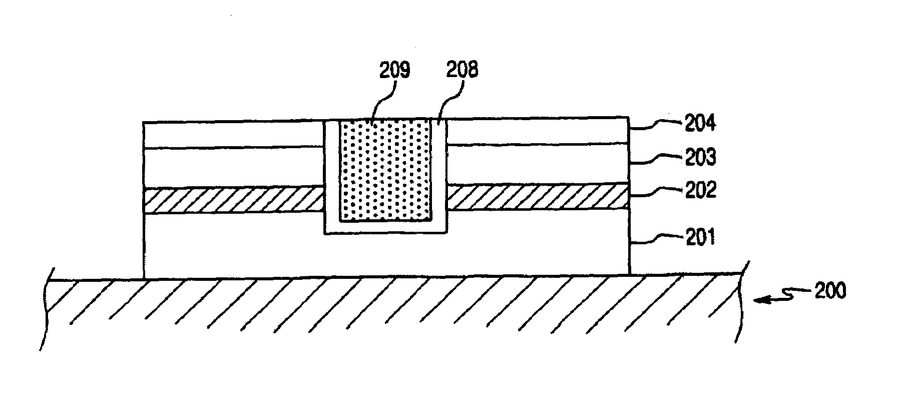
[0060]In the method for manufacturing the semiconductor device according to the present embodiment, an underlying insulating film 201 is disposed on a substrate 200 having a semiconductor device formed thereon, and a SiCN film 202, which will be an etch stop film at the stage of forming an interconnect groove, is deposited via plasma CVD thereon to a thickness of 50 nm. Then, a L-Ox™ film 203 is formed by an applying method to a thickness of 300 nm, and the baking processing is carried out within N2 atmosphere at 400 degree C. for 30 minutes. Subsequently, a SiO2 film 204 is deposited to a thickness of 100 nm (FIG. 9A). The deposition process of the SiO2 film 204 is carried out by employing a source gas containing SiH4 and N2O, and the volumetric flow rates of SiH4 and N2O are set to 2...

second embodiment

[0066]The present embodiment shows an embodiment, in which the present invention is applied to a dual-layer copper interconnect having a single damascene structure. FIG. 10 is a cross sectional view of structure of a semiconductor device according to the present embodiment. The semiconductor device according to the present embodiment has a configuration, in which a lower interconnect comprising a Cu film 209 is coupled to an upper interconnect comprising a Cu film 223 through a copper plug 228.

[0067]The lower interconnect comprising the Cu film 209 is formed in a multilayer films that include an underlying insulating film 201, a SiCN film 202, a L-Ox™ film 203 and a SiO2 film 204. Side surfaces and a bottom surface of the Cu film 209 are covered by Ta / TaN films 208.

[0068]The copper plug 228 is provided in a hole formed in multilayer films comprising a SiCN film 211 and a SiO2 film 212, and side surfaces and a bottom surface thereof are covered by Ta / TaN films 226.

[0069]The upper int...

example 1

[0085]In the present example, the moisture-absorption of an interconnect structure comprising a L-Ox™ film and a SiOC film, which form an interlayer insulating film, were examined by the pressure cooker test (PCT). The structure of the sample to be examined is shown in FIG. 15. The sample comprises a Cu single damascene structure including a low-k film, in which a lower copper interconnect is coupled to an upper copper interconnect through a via plug of Cu. A silicon substrate was employed for the substrate, and SiC-type films were employed for an etch stop film and a barrier insulating film. Further, a dual-layer structure of SiON / SiO2 (having an upper layer of SiON and a lower layer of SiO2) was employed for a cover film. Since the cover film was provided thereto, introduction of water from the top surface of the interconnect structure was inhibited.

[0086]The low-k films were employed for both the interconnect portion and the via portion of the interlayer insulating film. The empl...


PUM

PropertyMeasurementUnit
dielectric constantaaaaaaaaaa
densityaaaaaaaaaa
dielectric constantaaaaaaaaaa

Abstract

The present invention reduces the effective dielectric constant of the interlayer insulating film while inhibiting the decrease of the reliability of the semiconductor device, which otherwise is caused by a moisture absorption. A copper interconnect comprising a Cu film 209 is formed in multilayer films comprising a L-Ox™ film 203 and a SiO2 film 204. Since the L-Ox™ film 203 comprises ladder-shaped siloxane hydride structure, the film thickness and the film characteristics are stable, and thus changes in the film quality is scarcely occurred during the manufacturing process.

Description

[0001]This application is based on Japanese patent application NO. 2003-024281, the content of which is incorporated hereinto by reference.BACKGROUND OF THE INVENTION[0002]1. Field of the Invention[0003]The present invention relates to a technology for improving an adhesiveness of an interlayer insulating film employing an insulating material having a lower dielectric constant.[0004]2. Description of the Related Art[0005]Needs for achieving faster operation of semiconductor devices are growing in recent years, and in order to meet the needs, investigations for reducing the interconnect capacitance are actively conducted by replacing the conventional material for interlayer insulating film of the silicon oxide film (dielectric constant K=about 4.3) to a new material having lower dielectric constant. The insulating materials having lower dielectric constant include hydrogen silsesquioxane (HSQ), methyl silsesquioxane (MSQ), organic resin materials containing aromatic compounds or the ...

Claims


Application Information

Patent Timeline
Patent Type & Authority Patents(United States)
IPC IPC(8): H01L23/48H01L23/28H01L23/29H01L23/52H01L23/532C23C16/42H01L21/316H01L21/768H01L23/522
CPCH01L21/76829H01L21/76832H01L23/53238H01L23/53295H01L2924/0002H01L2924/00
Inventor USAMI, TATSUYAISHIGAMI, TAKASHIKUROKAWA, TETSUYAODA, NORIAKI
Owner RENESAS ELECTRONICS CORP
Why Eureka
Try Eureka