Wafer flatness evaluation method, wafer flatness evaluation apparatus carrying out the evaluation method, wafer manufacturing method using the evaluation method, wafer quality assurance method using the evaluation method, semiconductor device manufacturing method using the evaluation method and semiconductor device manufacturing method using a wafer evaluated by the evaluation method

a flatness evaluation and wafer technology, applied in the direction of semiconductor/solid-state device testing/measurement, printing, instruments, etc., can solve the problems of sfqr variation amount exceeding budget, unable to exhibit expected performance, and difficult to suppress cd variation within a sufficiently permissible rang

Active Publication Date: 2007-06-12
SHIN-ETSU HANDOTAI CO LTD +2
View PDF5 Cites 105 Cited by
  • Summary
  • Abstract
  • Description
  • Claims
  • Application Information

AI Technical Summary

Benefits of technology

[0066]FIG. 30 is a view showing one example of a quality assurance sheet obtained by a wafer quality assurance method according to a seventh embodiment of this invention;

Problems solved by technology

As a result, a wafer which is evaluated to have high flatness by use of the conventional evaluation standard, for example, evaluation standard by SFQR cannot exhibit an expected performance when the wafer is actually chucked on the holder of the exposure device.
Then, a focus variation amount exceeds the budget and it becomes difficult to suppress a CD variation within a sufficiently permissible range.

Method used


Image

  • Wafer flatness evaluation method, wafer flatness evaluation apparatus carrying out the evaluation method, wafer manufacturing method using the evaluation method, wafer quality assurance method using the evaluation method, semiconductor device manufacturing method using the evaluation method and semiconductor device manufacturing method using a wafer evaluated by the evaluation method
  • Wafer flatness evaluation method, wafer flatness evaluation apparatus carrying out the evaluation method, wafer manufacturing method using the evaluation method, wafer quality assurance method using the evaluation method, semiconductor device manufacturing method using the evaluation method and semiconductor device manufacturing method using a wafer evaluated by the evaluation method
  • Wafer flatness evaluation method, wafer flatness evaluation apparatus carrying out the evaluation method, wafer manufacturing method using the evaluation method, wafer quality assurance method using the evaluation method, semiconductor device manufacturing method using the evaluation method and semiconductor device manufacturing method using a wafer evaluated by the evaluation method

Examples


first embodiment

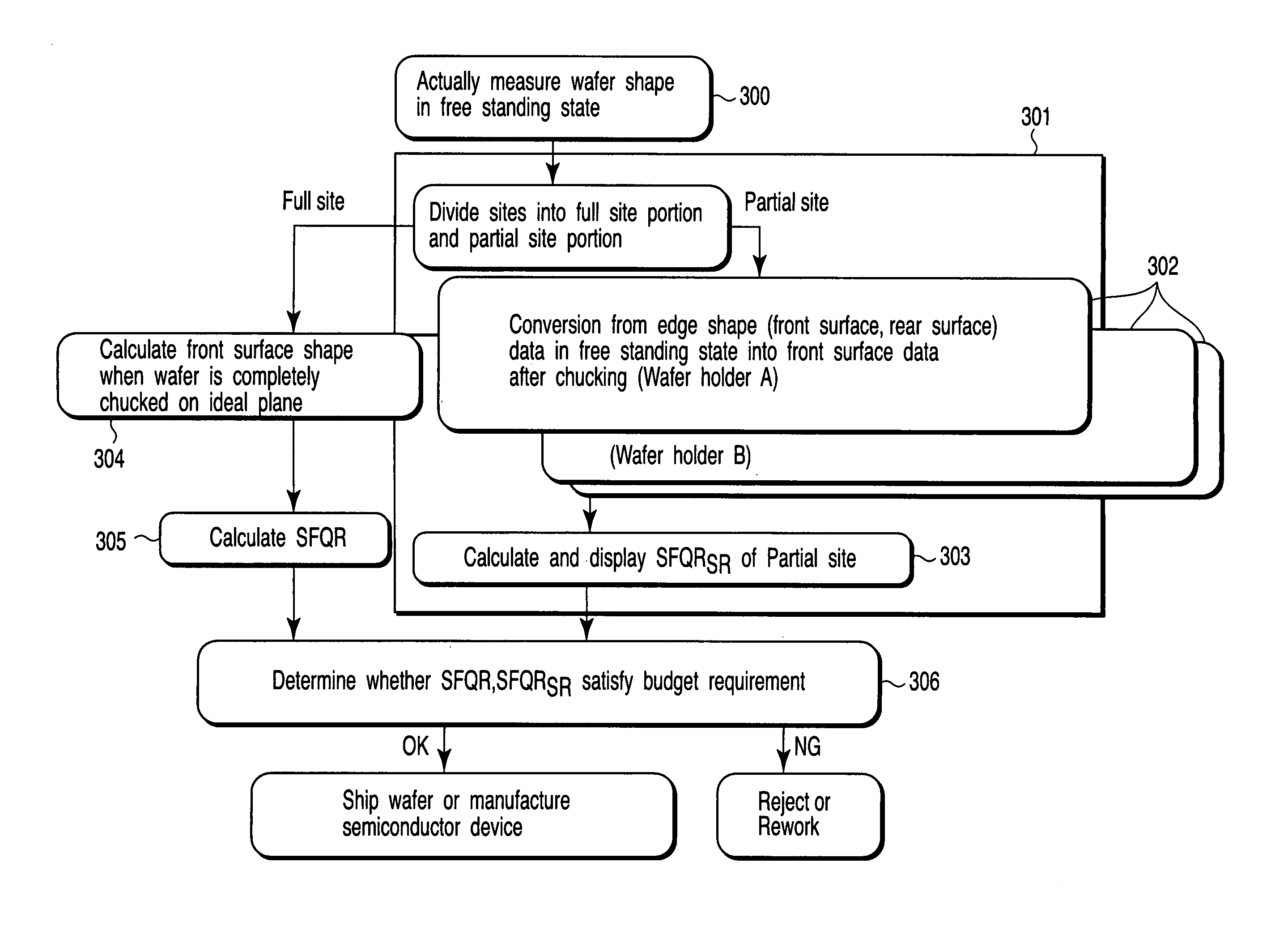
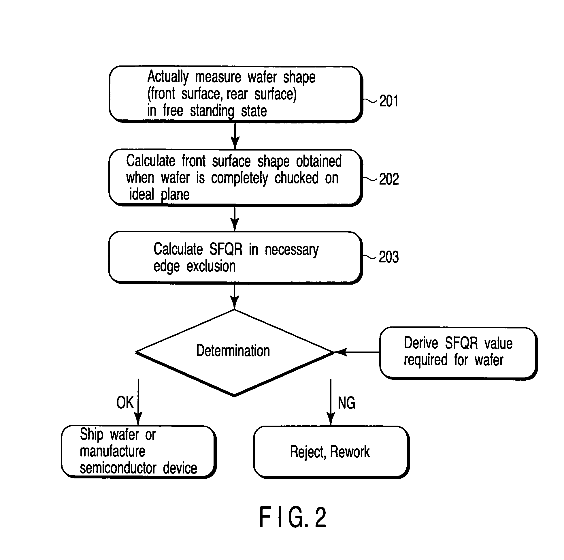
[0072]Prior to explanation of the first embodiment, definition of representative terms and a reference example used in this embodiment are explained with reference to FIGS. 1A to 1D and FIG. 2.

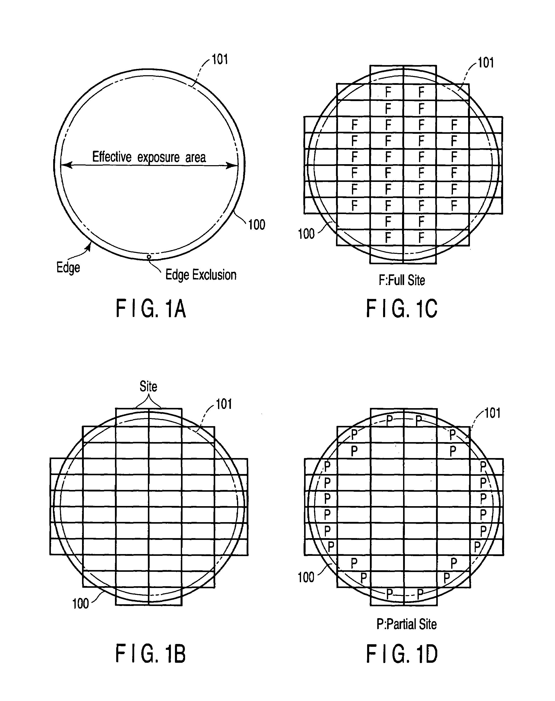
[0073]FIGS. 1A to 1D are plan views of a wafer.

[0074]It is desired to form an integrated circuit on the entire front surface of a wafer 100. However, actually, an effective integrated circuit is not formed on the entire surface of the wafer 100 and, as shown in FIG. 1A, an edge exclusion area with a width of approximately several mm from the edge of the wafer 100 is provided. An inside portion of the edge exclusion area is used as an effective exposure area and the effective integrated circuit is formed in the effective exposure area, for example. An outermost peripheral line for flatness evaluation set near the edge of the wafer 100 is set on a boundary line 101 between the edge exclusion area and the effective exposure area, for example.

[0075]FIG. 1B shows sites divided on the front surface ...

second embodiment

[0099]In the first embodiment, a method for calculating the flatness SFQRSR for each site based on the structure of the holder and the wafer shape measured in the steps 302, 303 and 306 shown in FIG. 3 and determining the flatness is used.

[0100]On the other hand, in the second embodiment, it is taken into consideration that the shape finally obtained in the wafer manufacturing process, for example, the free standing edge shape in the wafer surface is relatively constant in the radius vector direction (in a direction along the circumference of the wafer). Thus, the shape (at the upper and lower surfaces) of the wafer in freestanding state is determined, and a criterion is obtained for a condition in which the wafer chucked can have desired flatness SFQRSR. Then, the flatness SFQRSR that the wafer chucked has is evaluated.

[0101]FIG. 5 is a flow diagram showing a wafer flatness evaluation method according to the second embodiment of this invention.

[0102]As shown in FIG. 5, the surface ...

third embodiment

[0127]In the first and second embodiments, the wafer flatness evaluation method is selected according to a position of a site to be evaluated. In the third embodiment, the flatness degradation not in a position of the site but in a peculiar portion caused by the restriction on the wafer holder design is correctly evaluated.

[0128]FIG. 11A is a plan view of a wafer holder and FIG. 11B is a cross sectional view taken along the 11B-11B line of FIG. 11A.

[0129]As shown in FIGS. 11A and 11B, the holder has three wafer carrying / replacing lift pin holes 1101 in the central portion and the structure is made so as not to cause chucking on portions of the lift pin holes 1101. Unlike pin chuck portions 1102, the lift pin holes 1101 act as peculiar portions caused by the restriction on the wafer holder design. Uniform chucking cannot take place on sites lying on the lift pin holes 1101.

[0130]An influence given to the wafer flatness after chucking is checked for sites lying on the lift pin holes 1...


PUM


Abstract

There is disclosed a wafer flatness evaluation method includes measuring front and rear surface shapes of a wafer. The wafer front surface measured is divided into sites. Then, a flatness calculating method is selected according to a position of the site to be evaluated and flatness in the wafer surface is acquired.

Description

CROSS-REFERENCE TO RELATED APPLICATIONS[0001]This application is based upon and claims the benefit of priority from the prior Japanese Patent Application No. 2002-370502, filed Dec. 20, 2002, the entire contents of which are incorporated herein by reference.BACKGROUND OF THE INVENTION[0002]1. Field of the Invention[0003]This invention relates to a wafer flatness evaluation method, a wafer flatness evaluation apparatus which carries out the evaluation method, a wafer manufacturing method using the evaluation method, a wafer quality assurance method using the evaluation method, a semiconductor device manufacturing method using the evaluation method and a semiconductor device manufacturing method using a wafer evaluated by the evaluation method.[0004]2. Description of the Related Art[0005]The depth of focus gets closer to the limit as the pattern size of a semiconductor device is more miniaturized.[0006]In the 100 nm generation, it is important to suppress a variation in the focus whic...

Claims


Application Information

Patent Timeline
Patent Type & Authority Patents(United States)
IPC IPC(8): G03B27/58G03B27/42H01L21/66G01B11/30H01L21/027H01L21/302H01L21/461
CPCG01B11/306G01B21/30H01L22/12H01L2924/0002H01L2924/00
Inventor FUJISAWA, TADAHITOINOUE, SOICHIKOBAYASHI, MAKOTOICHIKAWA, MASASHIHAGIWARA, TSUNEYUKIKODAMA, KENICHI
Owner SHIN-ETSU HANDOTAI CO LTD
Why Eureka
Try Eureka