Optical functional film, method of forming the same, and spatial light modulator, spatial light modulator array, image forming device and flat panel display using the same
- Summary
- Abstract
- Description
- Claims
- Application Information
AI Technical Summary
Benefits of technology
Problems solved by technology
Method used
Image
Examples
Embodiment Construction
[0050]Hereinafter, an embodiment of the invention will be described with reference to the figures.
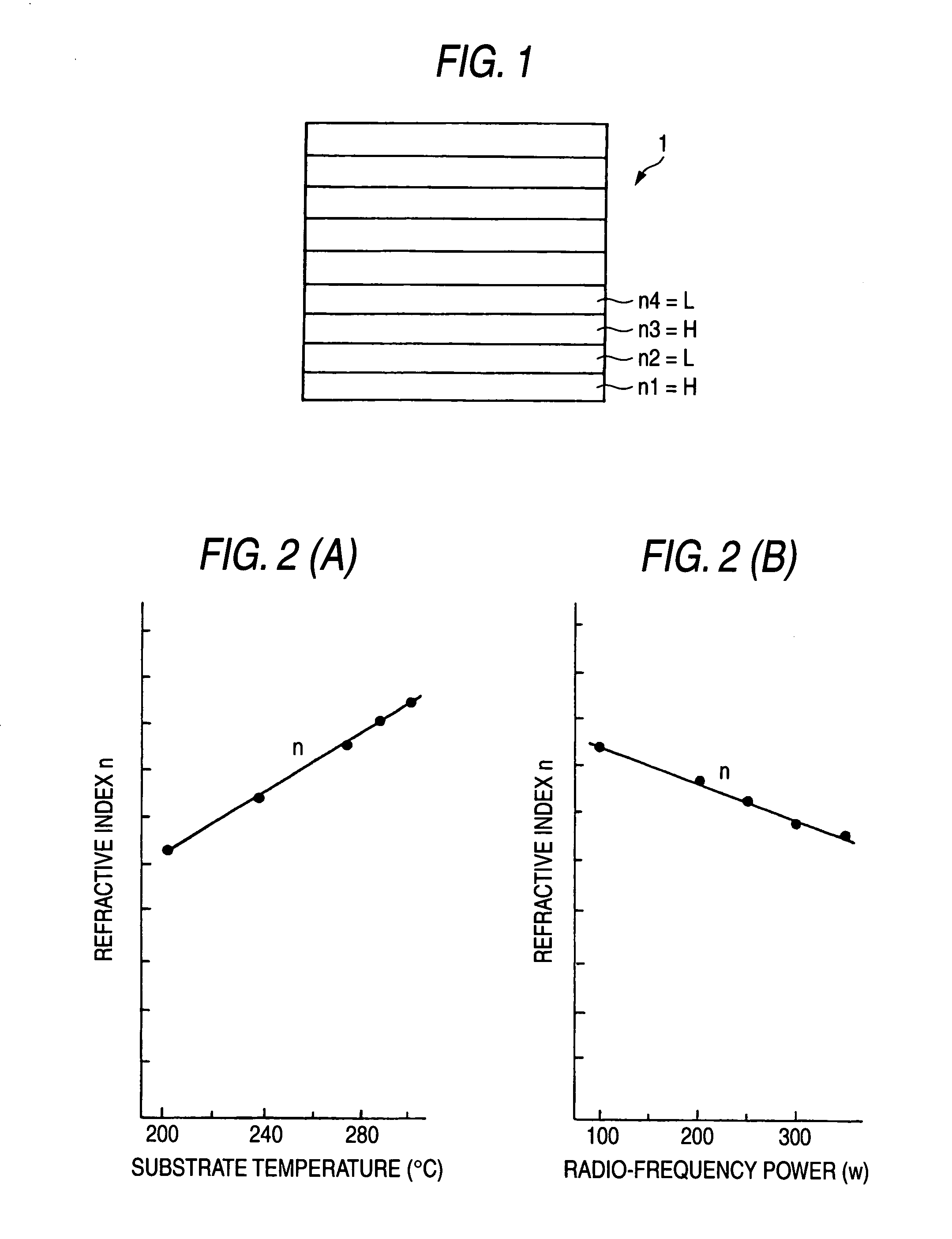
[0051]FIG. 1 is a section view of an optical functional film of the embodiment of the invention.
[0052]Referring to FIG. 1, 1 denotes a dielectric multilayer film mirror configuration which is stackingly formed with using a same material such as SiNx as a film material. In the specification, the term “same material” means that the same principal material is used in film growing processes, and “films made of a same material” means films made of same kinds of elements. In the case where dielectric films are to be formed by the plasma CVD method with using SiNx as a dielectric material, a silane gas and an ammonia gas are used as source gases, hydrogen and nitrogen are used as additive gases, and the gases are decomposed by an RF (radio-frequency) power to form thin films. In this case, the principal material means the silane gas and the ammonia gas serving as the source gases. In place of ...
PUM
 Abstract
Description
Claims
Application Information


