Method and apparatus for measuring thickness of a material

a technology of thickness measurement and material, applied in the direction of measuring devices, instruments, using optical means, etc., can solve the problems of optical interference outside the measured material rather than within, thinness of semiconductors which are thinner than the typical wafer thickness of 200 microns or more, and are currently difficult to measur

Active Publication Date: 2007-06-19
FILMETRICS
View PDF19 Cites 16 Cited by
  • Summary
  • Abstract
  • Description
  • Claims
  • Application Information

AI Technical Summary

Problems solved by technology

Thicknesses of semiconductors which are thinner than the typical wafer thickness of 200 microns or more, however, currently are difficult to measure.
Their thinness makes them too fragile to touch mechanically.
Using this technique, optical interference occurs outside of the measured material rather than within it.

Method used


Image

  • Method and apparatus for measuring thickness of a material
  • Method and apparatus for measuring thickness of a material
  • Method and apparatus for measuring thickness of a material

Examples


Embodiment Construction

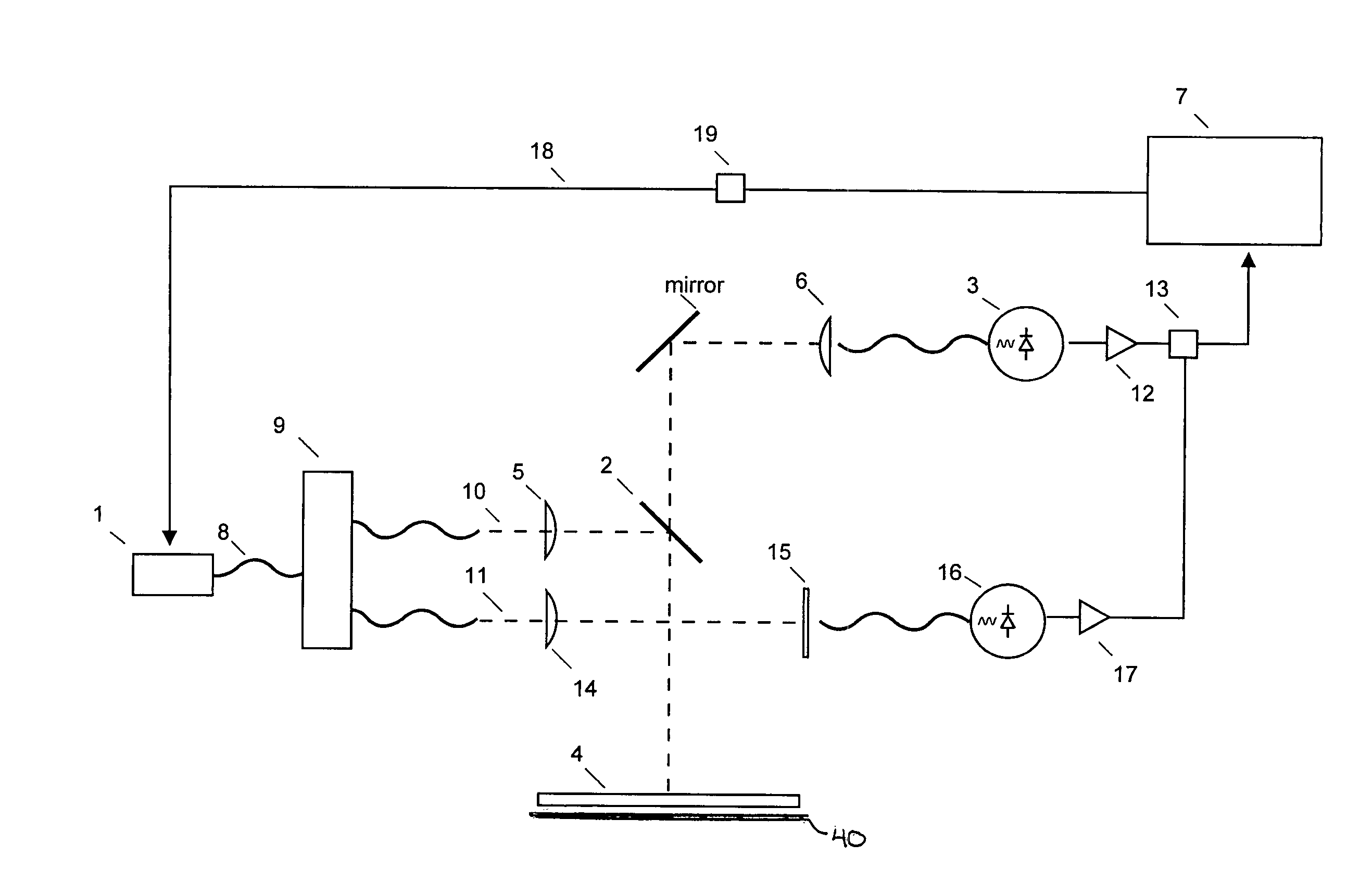
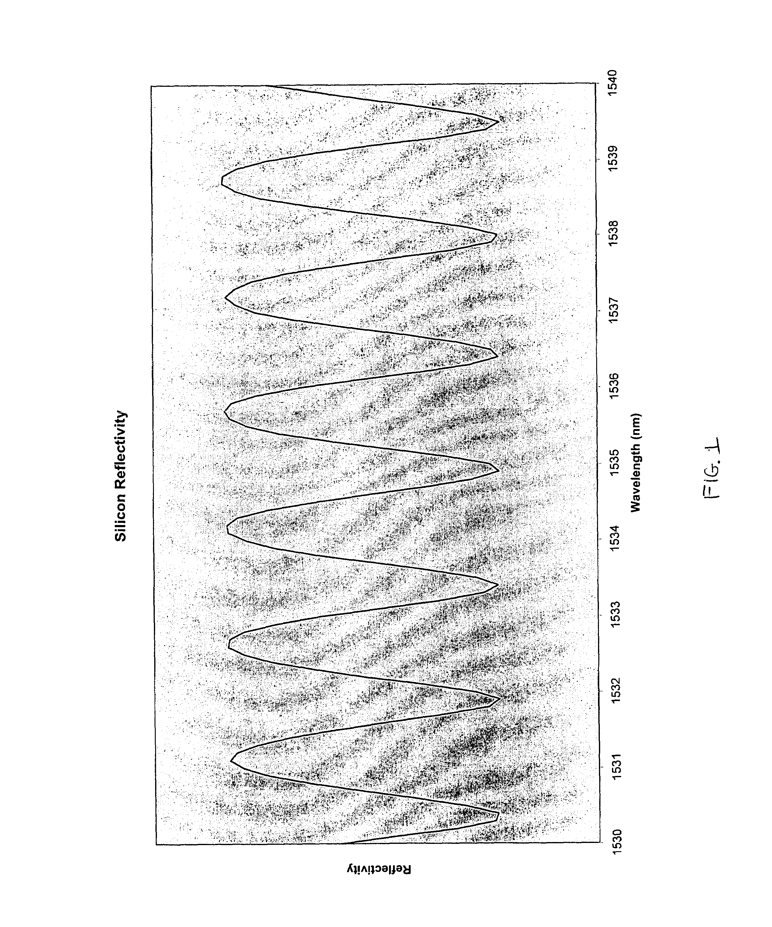
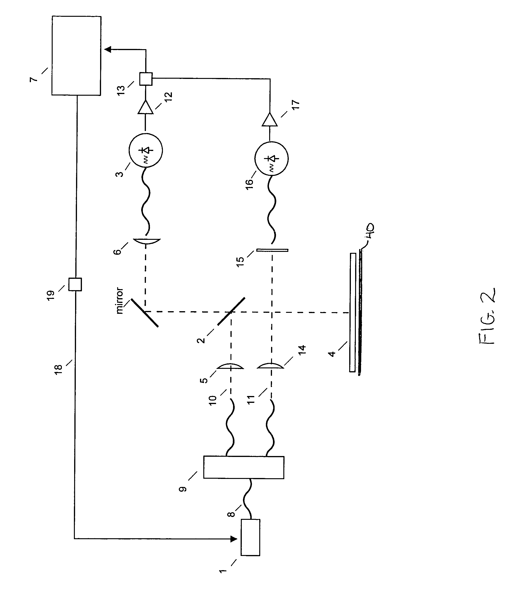
[0011]An objective of the invention is the determination of the thickness of a material quickly, accurately, and without contact, by means of measuring the material's reflectivity or transmissivity at multiple wavelengths at which the material is at least partially transparent.

[0012]The typical material is a silicon wafer which has been thinned, yet whose top and bottom surfaces remain co-planar enough to provide some optical interference between the surfaces. Preferably, the top and bottom surfaces vary less than 1 wavelength of light over an area having a 100 μm diameter. More preferably, the top and bottom surfaces vary less than 1 wavelength of light over the same area. Currently available measurement instruments which operate using visible light are unable to determine the thickness of the silicon, which is opaque to such light. This invention utilizes infrared light which is able to partially transmit through the material. Semiconductors become transparent at energies less tha...


PUM


Abstract

A method and apparatus for measuring wafers, thin films, or other planar layers are disclosed. This invention utilizes a tunable, monochromatic light source reflected from or transmitted through the layer to be measured. The wavelengths of light are selected such that the light is partially transmitted through the material to be measured so as optical interference is seen among the interfaces of the layer(s). The wavelengths are also controlled to sufficiently small increments to resolve these interference features. This apparatus relates to the need to monitor wafer thinning, film deposition, and other semiconductor device related processes.

Description

CLAIMS THE BENEFIT TO PROVISIONAL APPLICATION[0001]Pursuant to title 35, United States Code, Section 119(e) of the United States, this application claims benefit to the prior provisional patent application 60 / 486,371, filed on Jul. 11, 2003, the entire disclosure of which is hereby incorporated-by-reference for all purposes.FIELD OF THE INVENTION[0002]The present invention relates to an optical spectroscopic measurement system used to precisely determine the thickness of a layer of material typically of a semiconductor wafer.BACKGROUND OF THE INVENTION[0003]Considerable interest exists in determining the thickness of thin films used in the manufacture of micro-electronic, micro-optic, and micro-mechanical devices. Such measurement devices typically utilize visible light and are used to measure films of thickness on the order of the wavelength of light or less. Measurement of thicker materials such as semiconductor wafers is generally done with mechanical means. Thicknesses of semico...

Claims


Application Information

Patent Timeline
Patent Type & Authority Patents(United States)
IPC IPC(8): G01B11/06
CPCG01B11/0625
Inventor HOUSER, GLENN
Owner FILMETRICS
Why Eureka
Try Eureka