High temperature and chemical resistant process for wafer thinning and backside processing

a technology of chemical resistance and wafer thinning, which is applied in the direction of basic electric elements, semiconductor/solid-state device manufacturing, electric devices, etc., can solve the problems of silicon oxide thermal deposition and curing that are not satisfying certain processes, and achieve the effect of facilitating mounting

Inactive Publication Date: 2007-06-19
KMG ELECTRONICS CHEM
View PDF8 Cites 15 Cited by
  • Summary
  • Abstract
  • Description
  • Claims
  • Application Information

AI Technical Summary

Benefits of technology

[0006]The process of the invention employs a high temperature and chemical resistant adhesive based upon a cured silicone resin and a special reactive solvent mixture used to dissolve and remove the resin once wafer fabrication is complete. In the process a mixture of silicone monomers is applied to semiconductor wafers, curing and bonding steps, substrate thinning and processing to temperatures exceeding 200° C., and demount and clean with a specialty chemical solution. The spin-coat application of resin is designed to planarize the surface and encapsulate the device topography. Planarization is required for uniformity during bonding (mounting) to the carrier and subsequent mechanical handling. Additionally, the cured silicone acts to protect the wafer front-side surface (i.e., device area) and support the down-force pressures and shear stresses associated with backside thinning as carried out on a grinding and polishing tool.
[0007]Following the spin-coat application of the silicone thermoset resin, curing is achieved by heating such as on a hot plate. The applied heat cross-links (cures) the thermoset adhesive to produce a uniform, smooth, chemical and thermal resistant coating. Depending upon the height extent of wafer topography, conditions of the spin-speed coating, and a need for further surface penetration or planarization, the process may be repeated to lay down a second resin layer. Once the wafer is fully planarized and cured, an additional thin layer is applied to wet the surface for mounting to the carrier. This layer remains uncured until mounting. Mounting is facilitated by bringing the wafer and carrier substrate (e.g., sapphire, silicon or other ceramic) into contact and applying heat and pressure. Once cured, the wafer exists as a mounted package and thinning may proceed.

Problems solved by technology

Traditional temporary mounting adhesives are thermoplastic polymers with typical melting points below 170° C. and are unsatisfactory for certain processes such as silicon oxide thermal deposition and the curing of high temperature organic dielectrics such as polyamide.

Method used


Image

  • High temperature and chemical resistant process for wafer thinning and backside processing
  • High temperature and chemical resistant process for wafer thinning and backside processing
  • High temperature and chemical resistant process for wafer thinning and backside processing

Examples


Embodiment Construction

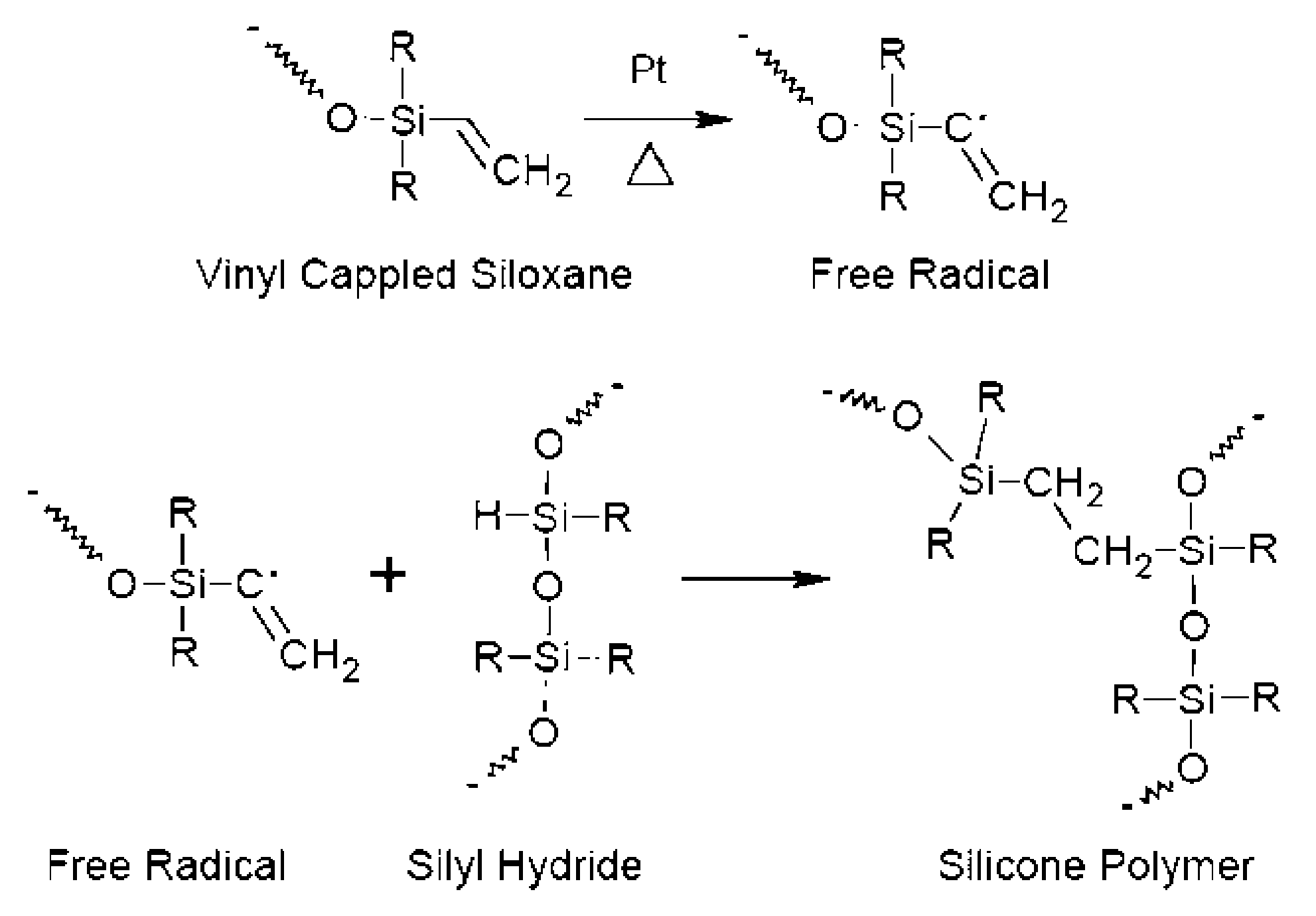
[0012]The invention utilizes a liquid form adhesive composition that is devised to be applied to semiconductor wafers by spin-on techniques, then cured, and subsequently used to mount wafers to rigid substrates. Essential to the invention is the provision of a high temperature and chemical resistant spin-on adhesive to provide high thermal resistance for subsequent thinning and backside wafer processing. The liquid adhesive is applied to the wafer front-side surface (i.e., device area) at specific conditions to achieve a defined thickness and to protect the device structures. Curing is done by thermal exposure, which cross-links the adhesive to produce a uniform, smooth, chemical and thermal resistant coating. Depending upon the wafer topography and a need for further surface penetration and planarization, the process may be repeated to lay down a second layer. Once the wafer is coated and cured, a thin layer is applied to the wafer to wet the surfaces for mounting. Mounting is faci...


PUM


Abstract

A process which uses a silicone resin to form a wafer-to-carrier bonded package that enables wafer thinning and backside processing while the cured resin exhibits high chemical and thermal resistance. The process is versatile in that the constructed wafer package allows for a wide range of chemical exposures to include dilute acid and base etchants, resist and residue strippers, electroplating chemistries, and also providing use in a range of deposition and etch processes that may exceed 300° C. The process utilizes a mixture of silicone monomers that when applied to semiconductor wafers by a spin-coat application, the result is a planarization of the front side device area, and when a subsequent thin coat is applied will facilitate bonding of the wafer-to-carrier package when heat and pressure are applied. The cured silicone bonded wafer-to-carrier package allows for wafer thinning consistent to industry objectives. Backside processing may include thermal oxide deposition, installed vias, and subsequent metallization in plating baths. Upon completion of a thinned and processed wafer, detachment occurs as described in prior art. Specialty chemical systems which completely dissolves the cured silicone and allows the wafer substrate to be easily rinsed and dried and become available for subsequent processing or final dicing and packaging.

Description

[0001]This invention relates to a process that uses a silicone blend adhesive system to facilitate the processing of semiconductor wafers. More specifically, the invention relates to a process that enables wafer processing at temperatures exceeding 200° C. where the high temperature and chemically resistant silicone resin is used as a temporary bonding adhesive to mount the wafer to a carrier substrate. Once the wafer is mounted, several semiconductor processes may be carried-out to include thinning, plasma etching, stripping, and in some cases, metallization. Once complete, the cured silicone resin is dissolved and removed with the use of a special reactive solvent mixture designed specifically to react and cleave the cross-linking which occurs in cured silicone polymers.BACKGROUND OF THE INVENTION[0002]Consistent with the design pressures of the semiconductor industry, there is a need to reduce the ever increasing heat build-up generated from higher power circuits that are smaller...

Claims


Application Information

Patent Timeline
Patent Type & Authority Patents(United States)
IPC IPC(8): H01L21/31
CPCH01L21/2007H01L21/3065
Inventor MOORE, JOHN C.SMITH, ALEXANDER C
Owner KMG ELECTRONICS CHEM
Why Eureka
Try Eureka