Methods and Apparatus For Thinning, Testing And Singulating A Semiconductor Wafer

a technology of semiconductor wafers and methods, applied in the direction of individual semiconductor device testing, semiconductor/solid-state device testing/measurement, instruments, etc., can solve the problem of not packaging integrated circuits that cannot perform as desired

Active Publication Date: 2010-06-10
TRANSLARITY INC
View PDF13 Cites 15 Cited by
  • Summary
  • Abstract
  • Description
  • Claims
  • Application Information

AI Technical Summary

Problems solved by technology

In this way, integrated circuits that cannot perform as desired are not packaged, or otherwise incorporated into finished products.

Method used


Image

  • Methods and Apparatus For Thinning, Testing And Singulating A Semiconductor Wafer
  • Methods and Apparatus For Thinning, Testing And Singulating A Semiconductor Wafer
  • Methods and Apparatus For Thinning, Testing And Singulating A Semiconductor Wafer

Examples


Embodiment Construction

[0027]Reference herein to “one embodiment”, “an embodiment”, or similar formulations, means that a particular feature, structure, operation, or characteristic described in connection with the embodiment, is included in at least one embodiment of the present invention. Thus, the appearances of such phrases or formulations herein are not necessarily all referring to the same embodiment. Furthermore, various particular features, structures, operations, or characteristics may be combined in any suitable manner in one or more embodiments.

Terminology

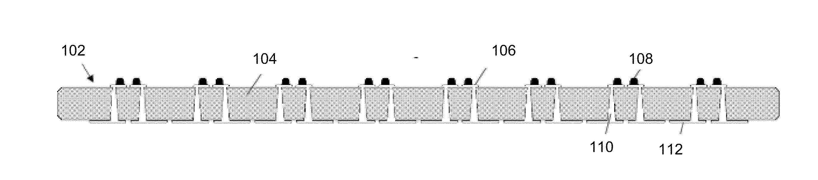
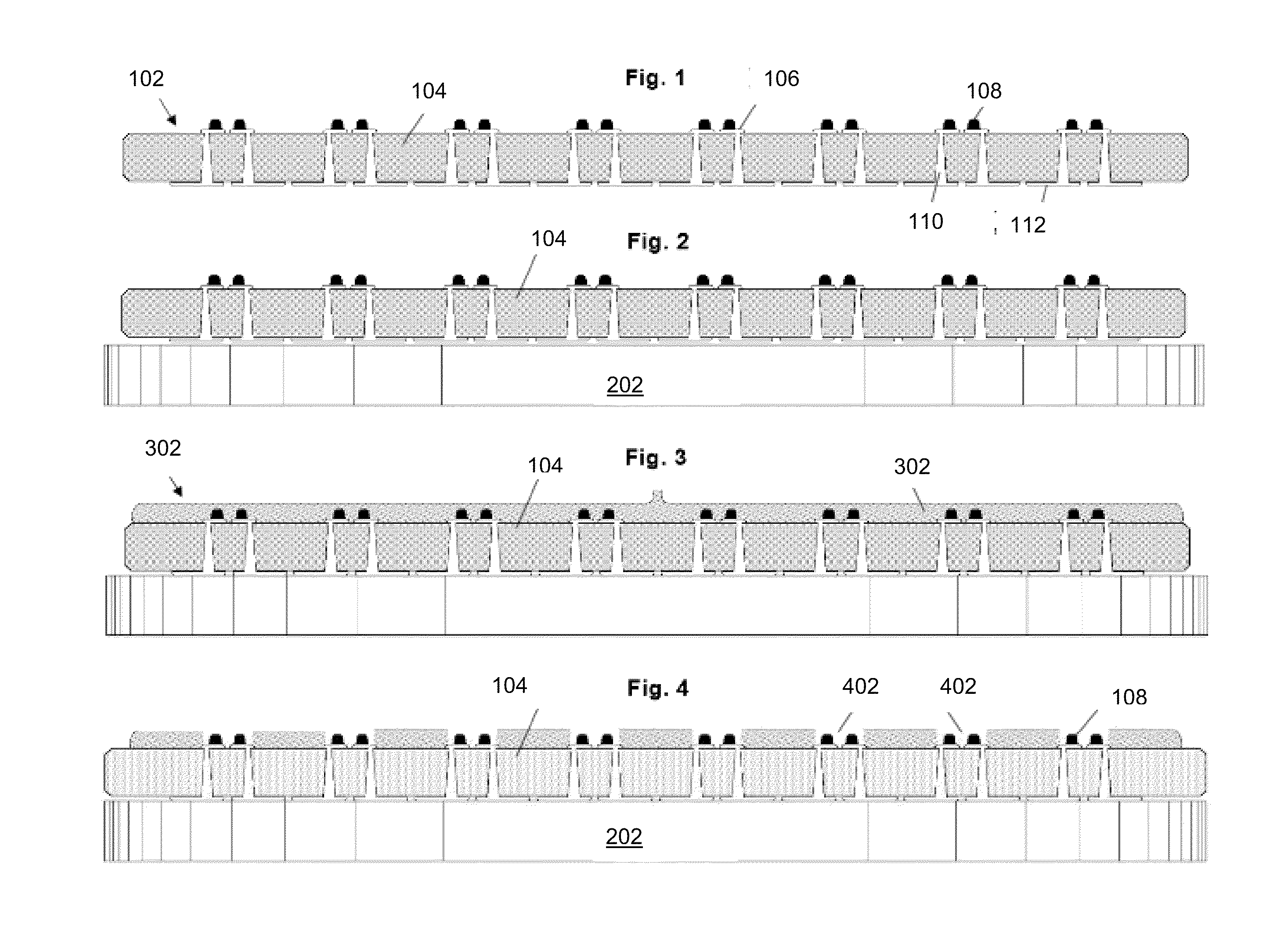
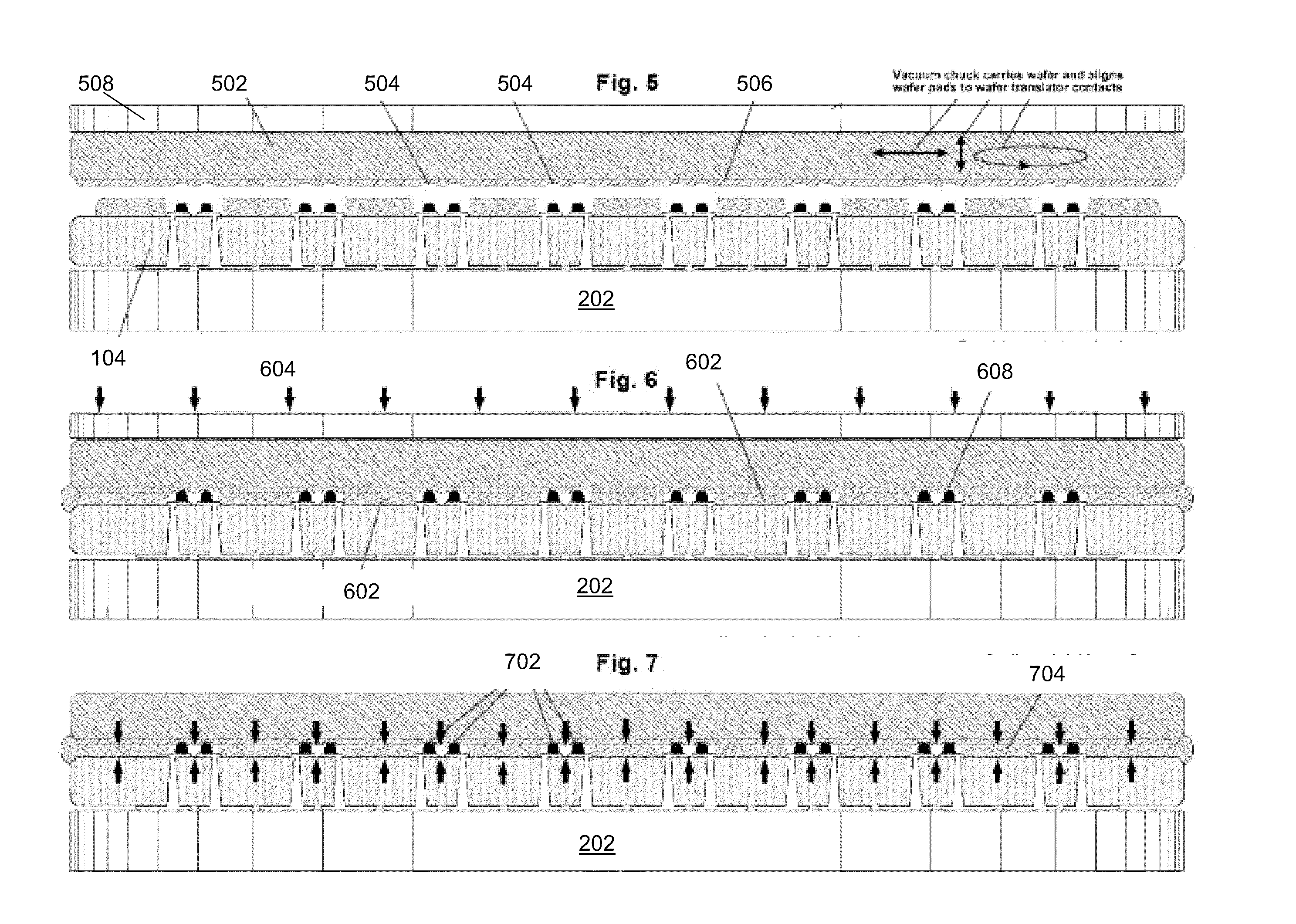
[0028]Pad refers to a metallized region of the surface of an integrated circuit, which is used to form a physical connection terminal for communicating signals to and / or from the integrated circuit.

[0029]The expression “wafer translator” refers to an apparatus facilitating the connection of pads (sometimes referred to as terminals, I / O pads, contact pads, bond pads, bonding pads, chip pads, test pads, or similar formulations) of unsingulated i...


PUM


Abstract

A wafer translator is provided with a patterned layer of wafer bonding thermoset plastic and is removably attached with a wafer so as to form a wafer/wafer translator pair. The wafer translator acts as a mechanical support during a thinning process as well as during a wafer dicing operation. The singulated integrated circuits are then removed from the wafer translator. In some embodiments, wafer level testing of the integrated circuits on the wafer is performed subsequent to the wafer thinning process but before the wafer and wafer translator are separated. In other embodiments, wafer level testing of the integrated circuits on the wafer is performed subsequent to the wafer dicing operation but before the diced wafer and wafer translator are separated.

Description

RELATED APPLICATIONS[0001]This application claims the benefit of Provisional Application No. 61 / 113,507, filed 11 Nov. 2008, and entitled “A Method of Testing Thinned And Singulated Die At The Wafer Level”, the entirety of which is hereby incorporated by reference.FIELD OF THE INVENTION[0002]The present invention relates generally to semiconductor test equipment, and more particularly relates to methods and apparatus for providing electrical pathways between the pads of integrated circuits on a wafer and circuitry external to the wafer.BACKGROUND[0003]Advances in semiconductor manufacturing technology have resulted in, among other things, reducing the cost of sophisticated electronics to the extent that integrated circuits have become ubiquitous in the modern environment.[0004]As is well-known, integrated circuits are typically manufactured in batches, and these batches usually contain a plurality of semiconductor wafers within and upon which integrated circuits are formed through a...

Claims


Application Information

Patent Timeline
Patent Type & Authority Applications(United States)
IPC IPC(8): H01L21/66H01L21/762H01L21/78
CPCG01R1/07307G01R31/2889H01L21/76256H01L21/67H01L2924/014G01R31/2601H01L22/20H01L21/67253H01L21/6835H01L21/6838H01L21/78H01L22/14H01L2221/68327H01L2221/68381
Inventor JOHNSON, MORGAN T.
Owner TRANSLARITY INC
Why Eureka
Try Eureka