Symmetric non-intrusive and covert technique to render a transistor permanently non-operable

Active Publication Date: 2007-07-10
RAYTHEON CO +2
View PDF167 Cites 21 Cited by
  • Summary
  • Abstract
  • Description
  • Claims
  • Application Information

AI Technical Summary

Benefits of technology

[0014]It is an object of this invention to make reverse engineering even more difficult and, in particular, to use LDD regions of opposite type from the active areas resulting in a transistor that is always off when standard voltages are applied to the

Problems solved by technology

It is believed that this will make the reverse engineer's efforts all the more difficult in terms of making it very time co

Method used


Image

  • Symmetric non-intrusive and covert technique to render a transistor permanently non-operable
  • Symmetric non-intrusive and covert technique to render a transistor permanently non-operable
  • Symmetric non-intrusive and covert technique to render a transistor permanently non-operable

Examples


Example

[0025]Semiconductor device manufacturing employs many techniques, process steps, and technologies that are well known. These techniques, process steps and technologies vary with feature size, material composition and other specific device attributes. The following discussions are general discussions regarding modifications that may be made to the masks used in manufacturing a CMOS device. The discussions below are provided as examples only of possible embodiments of the presently disclosed technology.

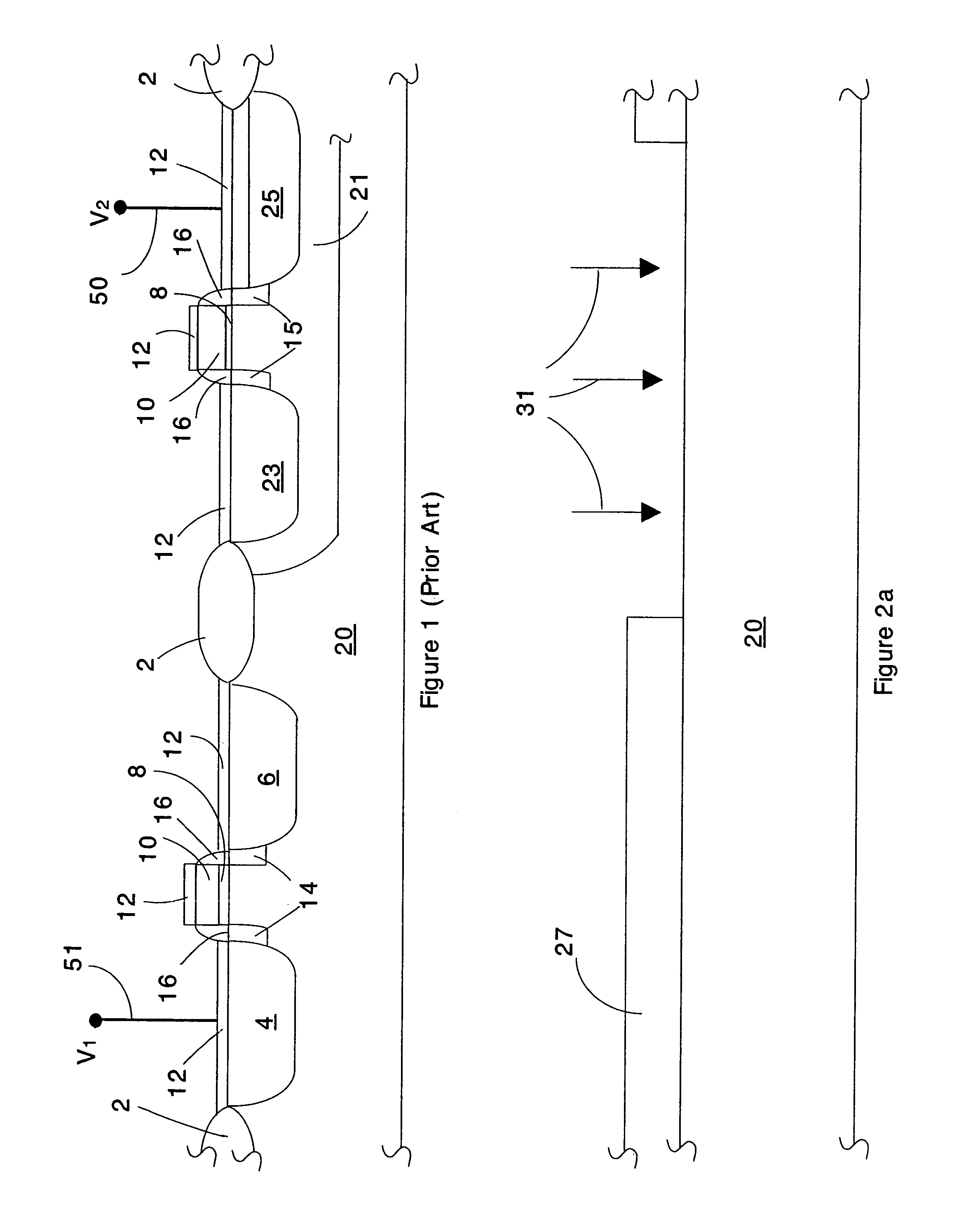
[0026]FIG. 2a depicts a substrate 20, for purposes of this discussion the substrate 20 is a p-type substrate; however the substrate could alternatively be a n-type substrate. A mask layer 27 is disposed over substrate 20 and photolithographically patterned to act as a mask for subsequent implantation. The substrate 20 is then exposed to ions 31. Ions 31 are chosen such that the ions 31 will result is a well of opposite conductivity type to that of substrate 20 (e.g. a n-type well 21 for...


PUM


Abstract

A technique for and structures for camouflaging an integrated circuit structure. The technique including forming active areas of a first conductivity type and LDD regions of a second conductivity type resulting in a transistor that is always non-operational when standard voltages are applied to the device.

Description

CROSS REFERENCE TO RELATED APPLICATIONS[0001]This application is related to U.S. patent application Ser. No. 10 / 828,022 filed on Apr. 19, 2004 and entitled “Covert Transformation of Transistor Properties as a Circuit Protection Method”, the disclosure of which is incorporated herein by reference.TECHNICAL FIELD[0002]The present invention relates to integrated circuits (ICs) and semiconductor devices in general and their methods of manufacture wherein the integrated circuits and semiconductor devices employ camouflaging techniques which make it difficult for the reverse engineer to discern how the semiconductor device functions by rendering devices, which appear to be normally functioning devices, non-operable (i.e. OFF).RELATED ART[0003]The present invention is related to the following US patents and patent applications by some of the same inventors as the present inventors:[0004](1) U.S. Pat. Nos. 5,866,933; 5,783,375 and 6,294,816 teach transistors in a CMOS circuit that are conne...

Claims


Application Information

Patent Timeline
IPC IPC(8): H01L29/76H01L27/088H01L29/94H01L31/062
CPCH01L21/823814H01L27/0203Y10S257/90H01L23/573
Inventor CHOW, LAP-WAICLARK, JR., WILLIAM M.HARBISON, GAVIN J.YANG, PAUL OU
Owner RAYTHEON CO
Why Eureka
Try Eureka