

Power amplifier
a power amplifier and amplifier technology, applied in the direction of amplifiers, amplifiers with semiconductor devices only, amplifiers with semiconductor devices, etc., can solve the problem of insufficient high efficiency
- Summary
- Abstract
- Description
- Claims
- Application Information
AI Technical Summary
Benefits of technology
Problems solved by technology
Method used
Image

Examples
first embodiment
(First Embodiment)
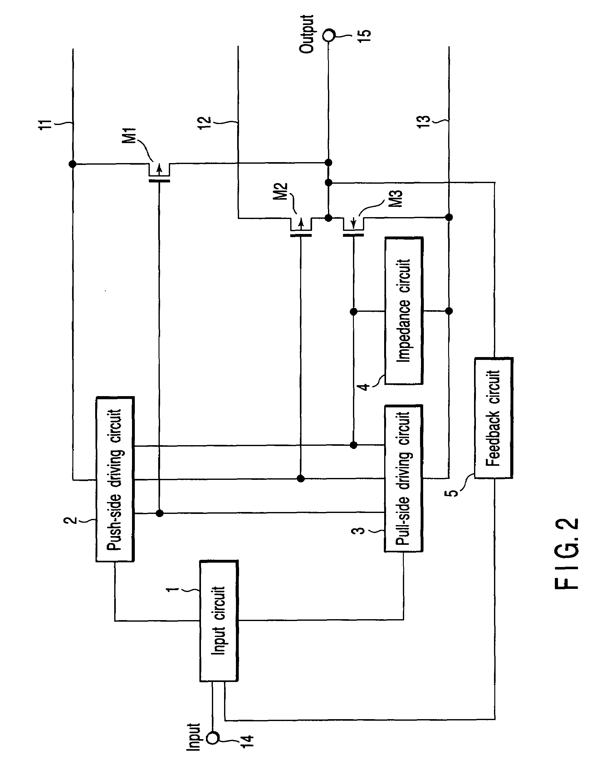
[0054]FIG. 2 is a circuit diagram (block diagram) that illustrates the basic structure of a power amplifier circuit, which is common to first to fifth embodiments of the present invention. An input circuit 1 receives an input signal from an input terminal and a feedback signal from a feedback circuit 5, amplifies the input signal and feedback signal, and delivers a first or a second control signal to a push-side driving circuit 2 or a pull-side driving circuit 3.
[0055]The push-side driving circuit 2 is supplied with power from a first power supply rail (power supply line) 11, and the pull-side driving circuit 3 is supplied with power from a third power supply rail (power supply line) 13. Normally, the first power supply rail 11 is connected to a power supply (Vcc) of the apparatus, and the third power supply rail 13 is connected to a ground potential (GND). Each of the push-side driving circuit 2 and pull-side driving circuit 3 has three driving signal output termi...
second embodiment
(Second Embodiment)
[0075]FIG. 4 is a circuit diagram of a power amplifier circuit according to a second embodiment of the invention. The second embodiment differs from the first embodiment in that the transistors of the push-side driving circuit 2 are composed of PMOS transistors Ma1, Ma2 and Ma3 and the transistors of the pull-side driving circuit 3 are composed of NMOS transistors Mb1, Mb2 and Mb3. The other parts are common to the first embodiment, and an overlapping description is omitted here.
[0076]The push-side driver transistors Ma1, Ma2 and Ma3 have a gate width / length (W / L) ratio or a gate area ratio of 4:1:2, and the pull-side driver transistors Mb1, Mb2 and Mb3 have a gate width / length (W / L) ratio or a gate area ratio of 1:1:1. Note that W is the gate width and L is the gate length.
[0077]Like the first embodiment, in the no-signal state in which no signal is input to the input terminal, the input circuit 1 is affected by the feedback circuit 5 so that a current of I may f...
third embodiment
(Third Embodiment)
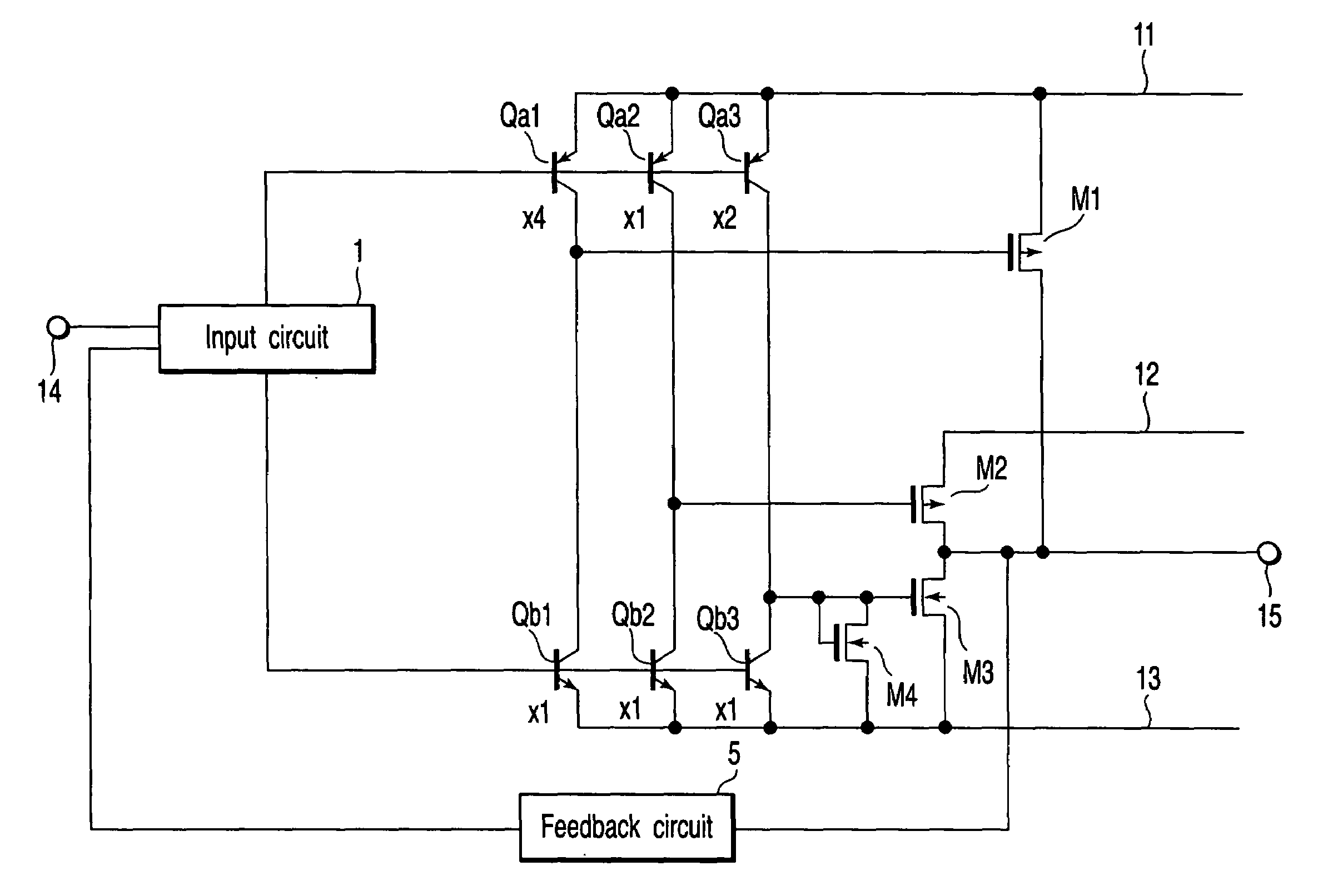
[0082]FIG. 5 is a circuit diagram of a power amplifier circuit according to a third embodiment of the invention. A first output transistor M1 is connected between the first power supply rail 11 and the output terminal 15. A second output transistor M2 is connected between the second power supply rail 12 and the output terminal 15, and a third output transistor M3 is connected between the output terminal 15 and the third power supply rail 13.
[0083]Driver transistors (bipolar transistors) Qa1, Qa2 and Qa3, which are driven by the input circuit 1 and function as the push-side driving circuit 2, have emitter areas with a ratio of 4:1:2, and their emitter resistances Ra1, Ra2 and Ra3 are set at ¼, 1 and ½, respectively. On the other hand, driver transistors (bipolar transistors) Qb1, Qb2 and Qb3, which are driven by the input circuit 1 and function as the pull-side driving circuit, have emitter areas with a ratio of 1:1:1, and their emitter resistances Rb1, Rb2 and Rb3 ...
PUM
 Abstract
Description
Claims
Application Information