Optical modulator

a technology of optical modulator and delay circuit, which is applied in the field of optical modulator, can solve the problems of increasing the cost of the entire optical modulator, increasing the setting space of the delay circuit, and complicated configuration, and achieves the effect of high phase difference accuracy and space saving

Inactive Publication Date: 2007-07-17
SUMITOMO OSAKA CEMENT CO LTD
View PDF13 Cites 28 Cited by
  • Summary
  • Abstract
  • Description
  • Claims
  • Application Information

AI Technical Summary

Benefits of technology

[0015]In accordance with the invention of claim 1, the branch element for branching a modulation signal into a plurality of modulation signals is formed and the delay line for generating the phase difference is formed in the middle of lines for applying the modulation signals branched by the branch element into the plurality of modulation electrodes. Therefore, a conventional delay circuit becomes unnecessary, and it becomes possible to apply the modulation signals with high phase difference accuracy. Further, it becomes possible to provide a cost-saving and space-saving optical modulator.
[0016]In accordance with the invention of claim 2, because the branch element is a divider or a T-type electrode, it is possible to incorporate the divider or the T-type electrode onto the substrate of the optical modulator, or onto the modulation signal relaying board positioned outside of the substrate. Therefore, it becomes possible to make the optical modulator structurally compact. Further, when the T-type electrode is formed on the substrate, the branch element can be formed at the same time as the modulation electrodes, which simplifies the production process as well.
[0017]In accordance with the invention of claim 3, because the divider or the T-type electrode is formed on the modulation signal relaying board positioned outside of the substrate, it becomes possible to provide a cost-saving and space-saving optical modulator only by connecting the relaying board to a conventional type of optical modulator substrate. It is also possible to prepare a plurality of relaying boards and select an appropriate relaying board in accordance with the frequency or intensity of the modulation signal used.
[0019]In accordance with the invention of claim 5, because the optical modulator is an SSB-type optical modulator or a duobinary-type optical modulator, a conventional delay circuit becomes unnecessary, and it becomes possible to apply the modulation signals with high phase difference accuracy, when the identical modulation signals having a predetermined phase difference are applied into the plurality of modulation electrodes, which is necessary for these optical modulators. Then, it becomes possible to provide a cost-saving and space-saving optical modulator.

Problems solved by technology

Therefore, there have been such problems as an increasing cost of the entire optical modulator, an increase of the setting space of delay circuit or the like.
Furthermore, because phase difference accuracy of precisely 90° cannot be obtained by a commercially available 90° hybrid, it is necessary to separately use a phase adjuster for fine adjustment, and this makes the configuration more complicated.
Thus, the number of components is increased and the configuration gets complicated.

Method used


Image

  • Optical modulator
  • Optical modulator
  • Optical modulator

Examples


second embodiment

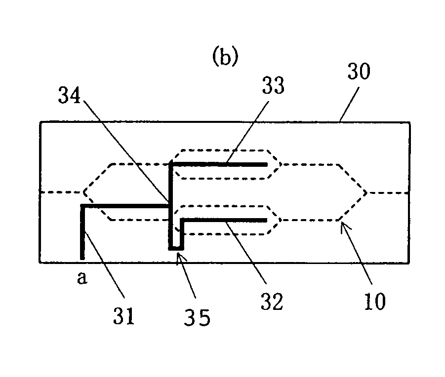
[0049]the present invention is shown in FIG. 3.

[0050]In FIGS. 3. a branch element such as a frequency divider is not provided outside of an SSB-type optical modulator 30. A T-type electrode 34, which is a branch element, and a delay line 35 are provided within the optical modulator 30, so as to apply identical modulation signals having a phase difference of 90° into modulation electrodes 32 and 33 as shown in FIG. 38. Reference numeral 31 denotes an introduction line of modulation signal into the T-type electrode 34.

[0051]As the configuration of the T-type electrode, it is preferable to match impedances of a junction as disclosed in Patent Document 1.

[0052][Patent Document 1]

[0053]Japanese Patent Laid-open Publication No. 2004-163859

[0054]By forming the T-type electrode and the delay line in combination on the substrate of the optical modulator 30 as shown in FIG. 3, the external branch element becomes unnecessary, and only one modulation signal is required to be inputted into the o...

third embodiment

[0055]Next, the present invention is shown in FIG. 4.

[0056]In the third embodiment, delay lines like the one shown in FIG. 2 are formed on relaying boards 41 and 43 provided outside of the substrate of an SSB-type optical modulator 40. In particular, the lengths of delay lines 42 and 44 respectively formed on the relaying boards 41 and 43 are differentiated, whereby a predetermined phase difference is generated. The use of relaying boards as stated above enables the conventional type of optical modulator shown in FIG. 1 to be used as the SSB-type optical modulator 40.

[0057]A plurality of relaying boards with delay lines of different lengths may be prepared as the relaying board 41 or 43, and combined in accordance with the necessary phase difference. The SSB-type optical modulator 40, relaying boards 41 and 43 may be housed in one case to be a single module. In this case, SSB modulation can be achieved by guiding two in-phase modulation signals generated by the frequency divider 8 a...

fourth embodiment

[0058]the present invention is shown in FIG. 5.

[0059]The fourth embodiment uses a relaying board 51 provided outside of the substrate of an SSB-type optical modulator 50 like the third embodiment. A T-type electrode 52 formed on the relaying board 51 allows omission of the frequency divider 8 of FIG. 4A. In the fourth embodiment, the delay line 23 is provided within the SSB-type optical modulator 50 like the first embodiment shown in FIG. 2. The use of such relaying board 51 enables only one modulation signal to be inputted.

[0060]By forming a delay line 55 like the delay line 44 in FIG. 4B as well as the T-type electrode 54 on a relaying board 53 as shown in FIG. 5C, the delay line 55 on the relaying board 53 may be endowed with the delay function of the delay circuit 23 partly or entirely.

[0061]Next, a method of adjusting the delay amount of the relaying board is explained.

[0062]When operating frequencies are different, it is necessary to change the delay amount in accordance with ...


PUM

PropertyMeasurementUnit
phaseaaaaaaaaaa
specific phase differenceaaaaaaaaaa
specific phaseaaaaaaaaaa

Abstract

The present invention provides a cost-saving and space-saving optical modulator enabling application of modulation signals with high phase difference accuracy without using a separate component for generating a phase difference outside of the optical modulator, when identical modulation signals having a predetermined phase difference are applied into a plurality of modulation electrodes.An optical modulator 20 including a substrate with an electro-optic effect, a plurality of optical waveguide sections 10 formed on the substrate, and a plurality of modulation electrodes 21 and 22 for modulating lights passing through the optical waveguide sections, and into which identical modulation signals having a predetermined phase difference are applied, wherein a branch element for branching a modulation signal into a plurality of modulation signals is formed, and a delay line for generating the phase difference is formed in the middle of lines for applying the modulation signals branched by the branch element into the plurality of modulation electrodes.

Description

BACKGROUND OF THE INVENTION[0001](1) Field of the Invention[0002]The present invention relates to an optical modulator, and in particular to an optical modulator applying identical modulation signals having a predetermined phase difference into a plurality of modulation electrodes.[0003](2) Related Art Statement[0004]An optical modulation method for applying identical modulation signals having a predetermined phase difference (=time delay) into a plurality of modulation electrodes, such as an SSB (Single-Side band) modulation method, a duobinary modulation method or the like, has been conventionally utilized in the field of optical communications or optical measurement.[0005]An SSB-type optical modulator consists of two sub Mach-Zehnder structures. In order to obtain SSB modulation signals, two splitted RF-signals with 90° phase difference by using an electrical 90° hybrid are applied to two sub-MZs modulation electrode respectively.[0006]A dual-electrode Mach-Zehnder type optical m...

Claims


Application Information

Patent Timeline
Patent Type & Authority Patents(United States)
IPC IPC(8): G02F1/035
CPCG02F1/225
Inventor FUJITA, TAKAHISAOIKAWA, SATOSHI
Owner SUMITOMO OSAKA CEMENT CO LTD
Why Eureka
Try Eureka