CMP slurry for forming aluminum film, CMP method using the slurry, and method for forming aluminum wiring using the CMP method

a technology of aluminum wiring and slurry, which is applied in the direction of surface treatment compositions, abrasives, chemistry apparatus and processes, etc., can solve the problems of voids forming in aluminum patterns, damascene methods can substantially influence the electrical characteristics of aluminum wiring, and the technique is not well suited to highly integrated devices with extremely small pattern widths and extremely small gaps. , to achieve the effect of reducing the removal rate of silicon oxide film

Active Publication Date: 2007-07-24
SAMSUNG ELECTRONICS CO LTD
View PDF9 Cites 2 Cited by
  • Summary
  • Abstract
  • Description
  • Claims
  • Application Information

AI Technical Summary

Benefits of technology

[0013]According to a first aspect of the present invention, a chemical mechanical polishing (CMP) slurry is provided for use in the CMP of an aluminum film formed over a silicion oxide film. The CMP slurry includes a polishing agent, an oxidant, a pH control additive, and an oxide film removal retarder which reduces a removal rate of the silicon oxide film.
[0014]According to another aspect of the present invention, a chemical mechanical polishing (CMP) slurry is provided for use in the CMP of an aluminum film formed over a silicion oxide film. The CMP slurry includes a polishing agent, an oxidant, a pH control additive, an oxide film removal retarder which reduces a removal rate of the silicon oxide film, and a defect prevention agent which inhibits at least one of scratch defects and corrosion defects at a surface of the aluminum film.
[0017]According to another aspect of the present invention, a method is provided for treating an aluminum film formed over a silicon oxide layer. The method includes providing a slurry containing a polishing agent, an oxidant, a pH control additive, and an oxide film removal retarder which reduces a removal rate of the silicon oxide film, and performing a chemical mechanical polishing (CMP) of the aluminum film using the slurry.
[0018]According to another aspect of the present invention, a method is provided of treating an aluminum film formed over a silicion oxide film. The method includes providing a first slurry containing a polishing agent, an oxidant, a pH control additive, and an oxide film removal retarder which reduces a removal rate of the silicon oxide film, and performing a first chemical mechanical polishing (CMP) of the aluminum film using the first slurry. The method further includes providing a second slurry containing a polishing agent, an oxidant, a pH control additive, an oxide film removal retarder which reduces a removal rate of the silicon oxide film, and a defect prevention agent which inhibits at least one of scratch defects and corrosion defects at a surface of the aluminum film, and performing a second CMP of the aluminum film using the second slurry. The first slurry is devoid of the defect prevention agent contained in the second slurry.
[0019]According to another aspect of the present invention, a method is provided of forming an aluminum wiring. The method includes forming an inter metal dielectric (IMD) layer containing silicon oxide over a semiconductor substrate, patterning the IMD layer to define an aluminum wiring region, forming a metal barrier layer on the patterned IMD layer to obtain a resultant structure, and coating the resultant structure with an aluminum film. The method further includes providing a slurry containing a polishing agent, an oxidant, a pH control additive, and an oxide film removal retarder which reduces a removal rate of the silicon oxide film, and performing a chemical mechanical polishing (CMP) of the aluminum film using the slurry to form an aluminum wiring within the aluminum wiring region.
[0020]According to yet another aspect of the present invention, a method is provided of forming an aluminum wiring. The method includes forming an inter metal dielectric (IMD) layer containing silicon oxide over a semiconductor substrate, patterning the IMD layer to define an aluminum wiring region, forming a metal barrier layer on the patterned IMD layer to obtain a resultant structure, and coating the resultant structure with an aluminum film. The method further includes providing a first slurry containing a polishing agent, an oxidant, a pH control additive, and an oxide film removal retarder which reduces a removal rate of the silicon oxide film, and performing a first chemical mechanical polishing (CMP) of the aluminum film using the first slurry. The method still further includes providing a second slurry containing a polishing agent, an oxidant, a pH control additive, an oxide film removal retarder which reduces a removal rate of the silicon oxide film, and a defect prevention agent which inhibits at least one of scratch defects and corrosion defects at a surface of the aluminum film, and performing a second CMP of the aluminum film using the second slurry to form an aluminum wiring within the aluminum wiring region. The first slurry is devoid of the defect prevention agent contained in the second slurry.

Problems solved by technology

However, this technique is not well suited to highly integrated devices having extremely small pattern widths and extremely small gaps between patterns.
Also, voids can form in the aluminum patterns as a result of heat stress induced migration after thermal processing or electro-migration.
The CMP process of the damascene method can substantially impact electrical characteristics of the aluminum wiring.
Over etching can decrease of the surface area of the aluminum wiring, which results in an increased electrical resistance of the aluminum wiring, which in turn can decrease the signal speed of the semiconductor device.
As such, over etching of the aluminum wiring can result if these slurries are used in the fabrication of highly integrated devices having extremely small wiring dimensions.
Also, the use of EP-A5680 can result in defects such as scratches and corrosion on the surface of the aluminum film.
That is, scratch defects create a surface roughness on the aluminum film and are caused by the polishing agent contacting the surface of the aluminum film.
In severe cases, the scratch defect can form a pit in the surface of the aluminum film which can adversely affect device performance.
Corrosion can result when aluminum ions break away from the aluminum film by a chemical reaction with other materials.
These defects are generally the result of material characteristics of aluminum, i.e., relatively low hardness and low resistance to stress.
Scratches or corrosion on the aluminum film can reduce the reflective index of the aluminum film and decrease reliability of the aluminum wiring.
In some cases, these defects can lead to discontinuities (open circuits) in the aluminum wiring.
However, aluminum to silicon oxide removal rate selectivity of the CMP9003 slurry is relatively low, which as discussed above can lead to problems when using the slurry in the fabrication of highly integrated semiconductor devices.

Method used


Image

  • CMP slurry for forming aluminum film, CMP method using the slurry, and method for forming aluminum wiring using the CMP method
  • CMP slurry for forming aluminum film, CMP method using the slurry, and method for forming aluminum wiring using the CMP method
  • CMP slurry for forming aluminum film, CMP method using the slurry, and method for forming aluminum wiring using the CMP method

Examples


first embodiment

CMP Slurry of a First Embodiment

[0034]A slurry for CMP of an aluminum film according to a first embodiment of the present invention is a compound containing a polishing agent, an oxidant, a pH control additive, and an oxide film removal retarder which reduces a removal rate of a silicon oxide film.

[0035]Colloidal silica (SiO2) is a preferred polishing agent for the slurry of the first embodiment. Other exemplary compounds that can be alternatively or additionally used as a polishing agent are alumina (Al2O3), ceria (CeO2), mangania (MnO2), or zirconia (ZrO2), or a composite of two or more of these materials. The polishing agent should cause minimum scratching on the surface of the aluminum film during a CMP process, and accordingly, the polishing agent should preferably have a small and uniform particle size distribution. Colloidal silica meets this characteristic requirement. A desirable ratio of the polishing agent in the first slurry to a total weight of the first slurry is 2˜20 ...

first experiment

[0039]CMP equipment designated as F-REX 200 and manufactured by Ebara Co. was used for the experiments described herein. The polishing pads used were an IC 1000 pad for the top polishing pad and a SUBA 4 pad for the sub polishing pad. All experimental data were obtained under the following operating conditions: (1) contact pressure (polishing load) of the wafer to the polishing pad was 250 hPa, and (2) rotational speed of the polishing plate, to which the polishing pad was attached, was 80 rpm.

[0040]In order to observe the effect of the oxidants in the CMP process, a removal rate of an aluminum film, a removal rate of a PE-TEOS film (inter metal dielectric (IMD) layer), and a reflective index (RI) after a CMP process were measured with respect to different oxidants contained in respective CMP slurries. Each slurry contained 10 wt % colloidal silica, and oxidant concentration of each was 0.1 M. The results of the first experiment are summarized in Table 1. Referring to Table 1, in vi...

second experiment

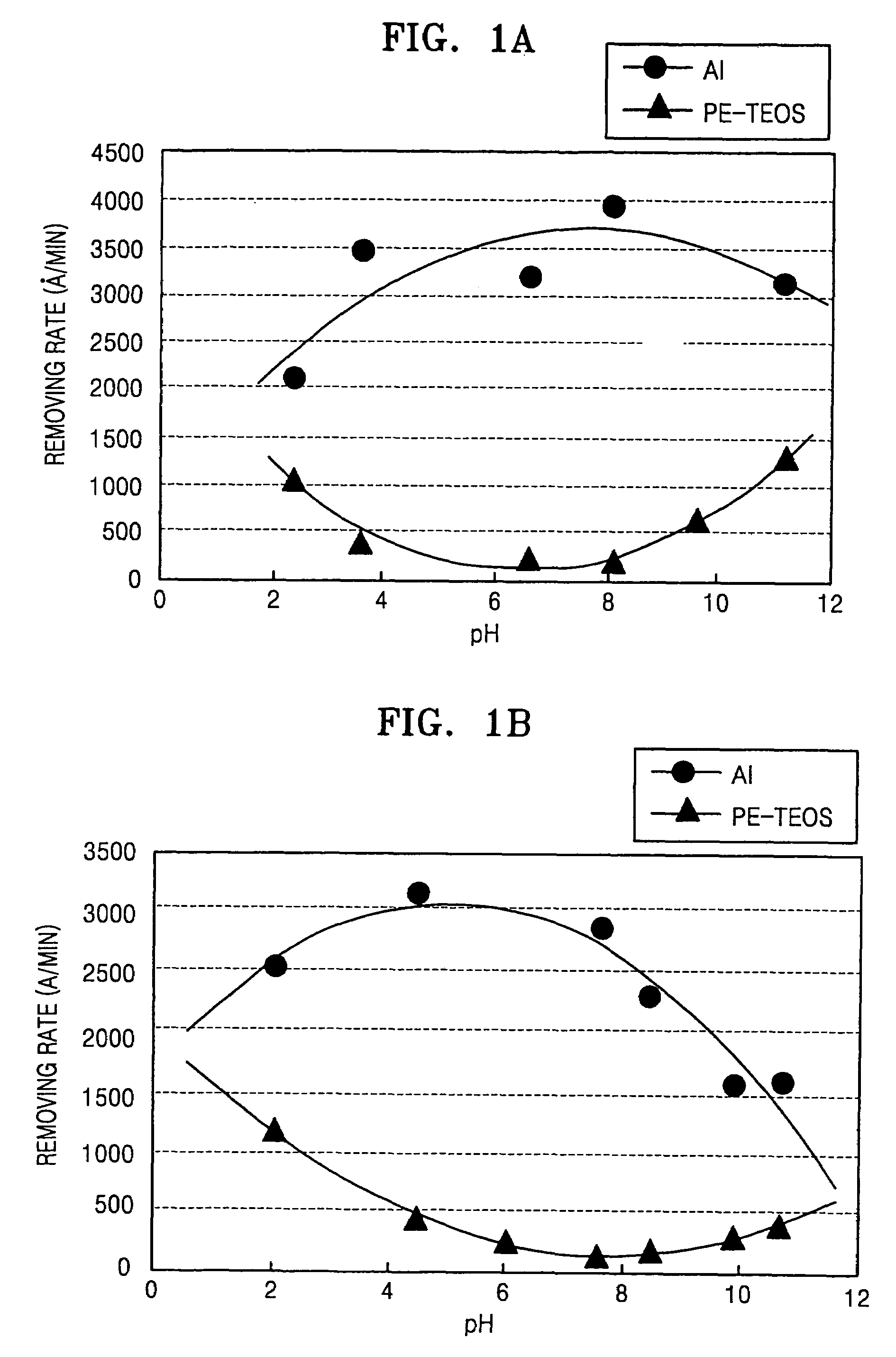
[0042]In order to observe the effect of the pH of the slurry in the CMP process, the removal rate of the aluminum film and the removal rate of the PE-TEOS film were measured while varying the pH of the slurry. Nitric acid and potassium hydroxide were used for the titrant, i.e., as additives for adjusting the pH. In the second experiment, a slurry having 10 wt % colloidal silica and 10 wt % hydrogen peroxide was prepared. Afterward, measurements were carried out using slurries in which the pH was controlled by adding the titrant. The results are summarized in Table 2 and depicted in FIG. 1A. Referring to Table 2 and FIG. 1A, the removal rate of the aluminum film and the silicon oxide film varied according to the pH of the slurry. In particular, when the pH of the first slurry is in a range of 4˜9, the removal rate selectivity of the aluminum film to the silicon oxide film is the greatest.

[0043]

TABLE 2RemovalRemovalRemoval raterate ofrate ofselectivitypH ofaluminum filmPE-TEOS film(Al...


PUM

PropertyMeasurementUnit
contact pressureaaaaaaaaaa
pHaaaaaaaaaa
leakage currentaaaaaaaaaa

Abstract

A first chemical mechanical polishing (CMP) slurry includes a polishing agent, an oxidant, a pH control additive, and an oxide film removal retarder which reduces a removal rate of the silicon oxide film. A second chemical mechanical polishing (CMP) slurry includes a polishing agent, an oxidant, a pH control additive, an oxide film removal retarder which reduces a removal rate of silicon oxide, and a defect prevention agent which inhibits scratch defects and / or corrosion defects at a surface of an aluminum film. In a one-step CMP process, either of the first or second slurry is used throughout CMP of an aluminum layer until an upper surface of an underlying silicon oxide layer is exposed. In a two-step CMP process, the first slurry is used in an initial CMP of the aluminum layer, and then the second slurry is used in a subsequent CMP until the upper surface of the underlying silicon layer is exposed.

Description

BACKGROUND OF THE INVENTION[0001]1. Field of the Invention[0002]The present invention generally relates to a chemical mechanical polishing (CMP) slurry and to a method of using the CMP slurry. More particularly, the present invention relates to a CMP slurry for use in polishing of an aluminum film, to a CMP method using the slurry, and to a method of forming an aluminum wiring using the CMP method.[0003]A claim of priority is made to Korean Patent Application No. 2003-70281, filed on Oct. 9, 2003 in the Korean Intellectual Property Office, which is incorporated herein in its entirety by reference.[0004]2. Description of the Related Art[0005]Aluminum is commonly used as the conductive material forming wirings and / or conductive plugs in semiconductor devices. Herein, the term “aluminum” is inclusive of aluminum alloys in which aluminum is the main component.[0006]Conventionally, an aluminum wiring or the like is formed by first depositing an aluminum film by sputtering or chemical vap...

Claims


Application Information

Patent Timeline
Patent Type & Authority Patents(United States)
IPC IPC(8): C09K13/00H01L21/304C09G1/02H01L21/321H01L21/768
CPCC09G1/02H01L21/3212H01L21/7684H01L21/304
Inventor PARK, JEONG-HEONLEE, JAE-DONGKIM, SUNG-JUNHONG, CHANG-KI
Owner SAMSUNG ELECTRONICS CO LTD
Why Eureka
Try Eureka