Method and composition for polishing a substrate

a technology of substrate and composition, applied in the direction of lapping machines, water dispersions, other chemical processes, etc., can solve the problems of uneven surface formation, undesirable residue retention, and residue dishing on the substrate surface, and achieve the effect of high removal ra

Inactive Publication Date: 2007-01-09
APPLIED MATERIALS INC
View PDF205 Cites 21 Cited by
  • Summary
  • Abstract
  • Description
  • Claims
  • Application Information

AI Technical Summary

Benefits of technology

[0011]Embodiments of the invention provide compositions and methods for removing conductive materials by an electrochemical mechanical polishing technique. In one aspect, a method is provided for processing a substrate having a conductive material layer disposed thereon including providing the substrate to a process apparatus comprising a first electrode and a second electrode with the substrate in electrical contact with the second electrode, wherein the substrate surface comprises conductive material layer disposed over narrow feature definitions and wide feature definitions, supplying a polishing composition between the first electrode and the substrate, wherein the polishing composition comprises an acid based electrolyte system, one or more chelating agents, greater than about 0.2 wt. % of one or more corrosion inhibitors, one or more inorganic or organic acid salts, one or more pH adjusting agents to provide a pH between greater than about 4.5 and about 7, and a solvent, wherein the polishing composition forms a passivation layer on the conductive material, abrading the passivation layer to expose a portion of the conductive material, applying a bias between the first electrode and the second electrode, and removing conductive material disposed over narrow feature definitions at a higher removal rate than conductive material disposed over wide feature definitions.
[0012]In one aspect, a method is provided for processing a substrate having a conductive material layer disposed thereon including providing the substrate to a process apparatus comprising a first electrode and a second electrode with the substrate in electrical contact with the second electrode, wherein the conductive material layer is disposed over narrow feature definitions and wide feature definitions, supplying a polishing composition between the first electrode and the substrate, wherein the polishing composition forms a passivation layer on exposed conductive material, abrading the passivation layer to expose a portion of the conductive material, and applying power by a pulse modulation technique between the first electrode and the second electrode to remove conductive material disposed over narrow feature definitions at a higher removal rate than conductive material disposed over wide feature definitions.
[0013]In one embodiment, the polishing composition includes an acid based electrolyte system, one or more chelating agents, one or more corrosion inhibitors, one or more inorganic or organic acid salts, one or more pH adjusting agents to provide a pH between about 2 and about 10, and a solvent. The method further includes forming a protrusion of conductive material over the wide feature definitions. The method also further includes polishing the substrate by at least a chemical mechanical polishing process. The chemical mechanical polishing process may be a chemical mechanical polishing process or a second electrochemical mechanical polishing process.
[0014]The electrochemical mechanical polishing process may be performed in a process apparatus, such as a toll having one or more polishing stations adapted for electrochemical mechanical polishing processes. A platen for performing an electrochemical mechanical polishing process may include a polishing article, a first electrode and a second electrode, wherein the substrate is in electrical contact with the second electrode. The electrochemical mechanical polishing process may be performed on a first platen as described herein, the chemical mechanical polishing process may be performed on a conventional chemical mechanical polishing platen, and the second electrochemical mechanical polishing process may be performed on the same or different platen adapted for electrochemical mechanical polishing, such as the second platen as described herein.
[0015]In another aspect, a method is provided for processing a substrate having a conductive material layer disposed thereon over narrow feature definitions and wide feature definitions including removing conductive material disposed over narrow feature definitions at a higher removal rate than conductive material disposed over wide feature definitions by an electrochemical mechanical polishing technique and removing conductive material disposed over wide feature definitions at a removal rate greater than or equal to the removal rate of conductive material disposed over narrow feature definitions by at least a chemical mechanical polishing technique. The method may comprise polishing the substrate initially with an electrochemical mechanical process and then with a chemical mechanical polishing process or a second electrochemical mechanical process adapted to remove conductive material disposed over wide feature definitions at a removal rate greater than or equal to the removal rate of conductive material disposed over narrow feature definitions. The second electrochemical mechanical process may have a corrosion inhibitor concentration less than the first electrochemical mechanical process and / or have a pH less than the first electrochemical mechanical process.

Problems solved by technology

However, as the limits of circuit technology are pushed, the shrinking dimensions of interconnects in VLSI and ULSI technology have placed additional demands on processing capabilities.
However, materials deposited on the surface of a substrate to fill feature definitions formed therein often result in unevenly formed surfaces over feature definitions of variable density.
Polishing of surfaces with overburden may result in the retention of residues 50 from inadequate metal removal over narrow features.
Dishing of features and retention of residues on the substrate surface are undesirable since dishing and residues may detrimentally affect subsequent processing of the substrate.
For example, dishing results in a non-planar surface that impairs the ability to print high-resolution lines during subsequent photolithographic steps and detrimentally affects subsequent surface topography of the substrate, which affects device formation and yields.
Dishing also detrimentally affects the performance of devices by lowering the conductance and increasing the resistance of the devices, causing device variability and device yield loss.
Residues may lead to uneven polishing of subsequent materials, such as barrier layer materials (not shown) disposed between the conductive material and the substrate surface.
Uneven polishing will also increase defect formation in devices and reduce substrate yields.

Method used


Image

  • Method and composition for polishing a substrate
  • Method and composition for polishing a substrate
  • Method and composition for polishing a substrate

Examples


example 1

[0115]A copper plated substrate was polished and planarized using the following polishing composition within a modified cell on a REFLEXION® system, available from Applied Materials, Inc. of Santa Clara, Calif. A substrate having a copper layer of about 11,500 Å thick on the substrate surface with a step height of about 6,000 Å was exposed to a polishing composition of:

[0116]about 6% by volume phosphoric acid;

[0117]about 2% by volume ethylenediamine;

[0118]about 2% by weight ammonium citrate;

[0119]about 0.3% by weight benzotriazole;

[0120]between about 2% and about 6% by volume of potassium hydroxide to provide a pH of about 5; and

[0121]deionized water, and

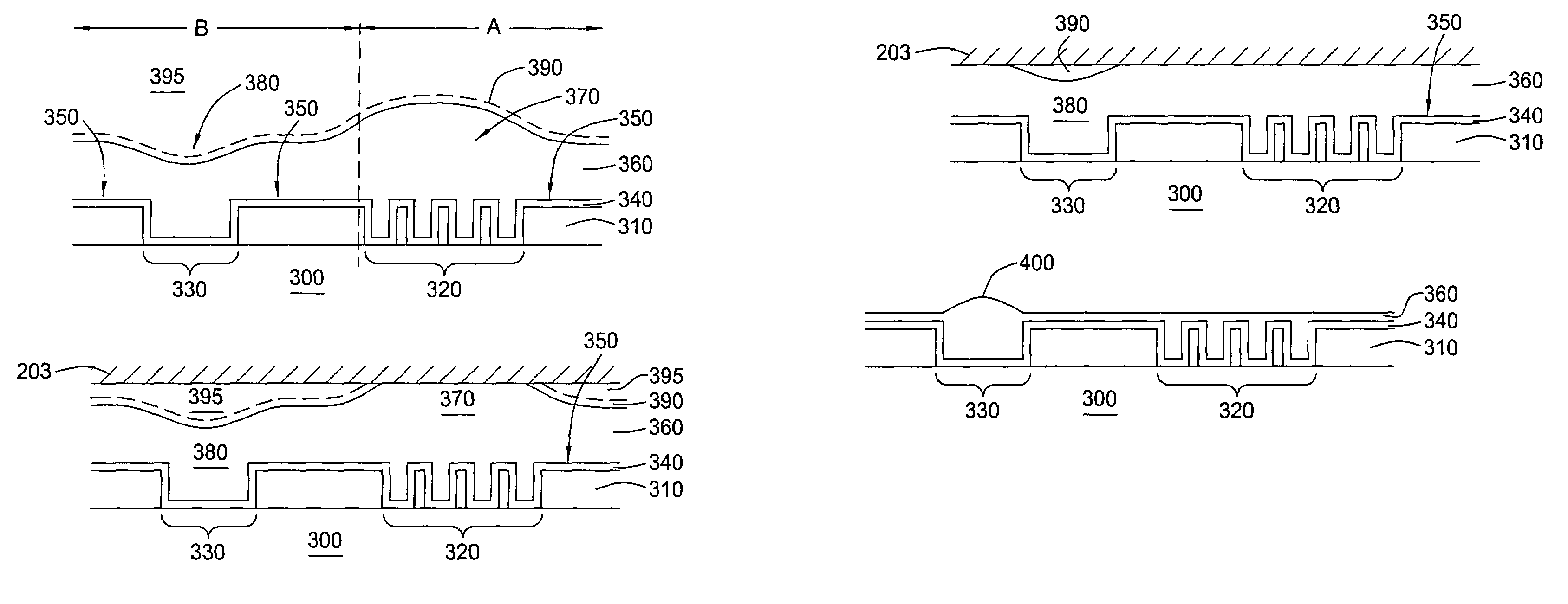
[0122]a polishing article was contacted with the substrate at about 0.2 psi at a bias of about 3 watts / volts was applied during the process. The substrate was polishing and examined. A protrusion height of about 4,000 Å was observed over wide feature definitions.

example 2

[0123]A copper plated substrate was polished and planarized using the following polishing composition within a modified cell on a REFLEXION® system, available from Applied Materials, Inc. of Santa Clara, Calif. A substrate having a copper layer of about 11,500 Å thick on the substrate surface with a step height of about 6,000 Å was exposed to a polishing composition of:

[0124]about 6% by volume phosphoric acid;

[0125]about 2% by volume ethylenediamine;

[0126]about 2% by weight ammonium citrate;

[0127]about 0.3% by weight benzotriazole;

[0128]between about 2% and about 6% by volume of potassium hydroxide to provide a pH of about 5; and

[0129]deionized water, and

[0130]a polishing article was contacted with the substrate at about 0.2 psi at a bias of about 3 watts / volts was applied by a pulse technique of 10 seconds on and 2 seconds off for 8 of cycles. The substrate was polishing and examined. A protrusion height of about 1,500 Å was observed over wide feature definitions.


PUM

PropertyMeasurementUnit
contact pressureaaaaaaaaaa
velocityaaaaaaaaaa

Abstract

Polishing compositions and methods for removing conductive materials from a substrate surface are provided. In one aspect, a method is provided for processing a substrate to remove conductive material disposed over narrow feature definitions formed in a substrate at a higher removal rate than conductive material disposed over wide feature definitions formed in a substrate by an electrochemical mechanical polishing technique. The electrochemical mechanical polishing technique may include a polishing composition comprising an acid based electrolyte system, one or more chelating agents, one or more corrosion inhibitors, one or more inorganic or organic acid salts, one or more pH adjusting agents to provide a pH between about 2 and about 10, and a solvent.

Description

CROSS-REFERENCE TO RELATED APPLICATIONS[0001]This application is a continuation-in-part of U.S. patent application Ser. No. 10 / 038,066, filed Jan. 3, 2002 now U.S. Pat. No. 6,811,680, entitled “Planarization Of Substrates Using Electrochemical Mechanical Polishing”, that claims priority to U.S. Provisional Patent Application Ser. No. 60 / 275,874, filed on Mar. 14, 2001, a continuation-in-part of U.S. patent application Ser. No. 10 / 032,275, filed Dec. 21, 2001 now U.S. Pat. No. 6,899,804, entitled “Electrolyte Composition And Treatment For Electrolytic Chemical Mechanical Polishing”, which applications are incorporated by reference herein, a continuation-in-part of co-pending U.S. patent application Ser. No. 10 / 378,097, filed Feb. 26, 2003, entitled “Method and Composition For Polishing a Substrate”, which claims priority to U.S. Provisional Patent Application Ser. No. 60 / 359,746, filed on Feb. 26, 2002, and a continuation-in-part of co-pending U.S. patent application Ser. No. 10 / 456,...

Claims


Application Information

Patent Timeline
Patent Type & Authority Patents(United States)
IPC IPC(8): B23H5/08B23H3/08B24B37/04C09G1/04C25F3/02H01L21/321H01L21/3213H01L21/768
CPCB23H3/08B23H5/08B24B37/0056B24B37/044B24B37/046H01L21/7684C25F3/02H01L21/3212H01L21/32125C09G1/04H01L21/32134C09G1/02C09K3/14
Inventor LIU, FENG Q.CHEN, LIANG-YUHTSAI, STAN D.DUBOUST, ALAINNEO, SIEW S.HU, YONGQIWANG, YANBUTTERFIELD, PAUL D.
Owner APPLIED MATERIALS INC
Why Eureka
Try Eureka