

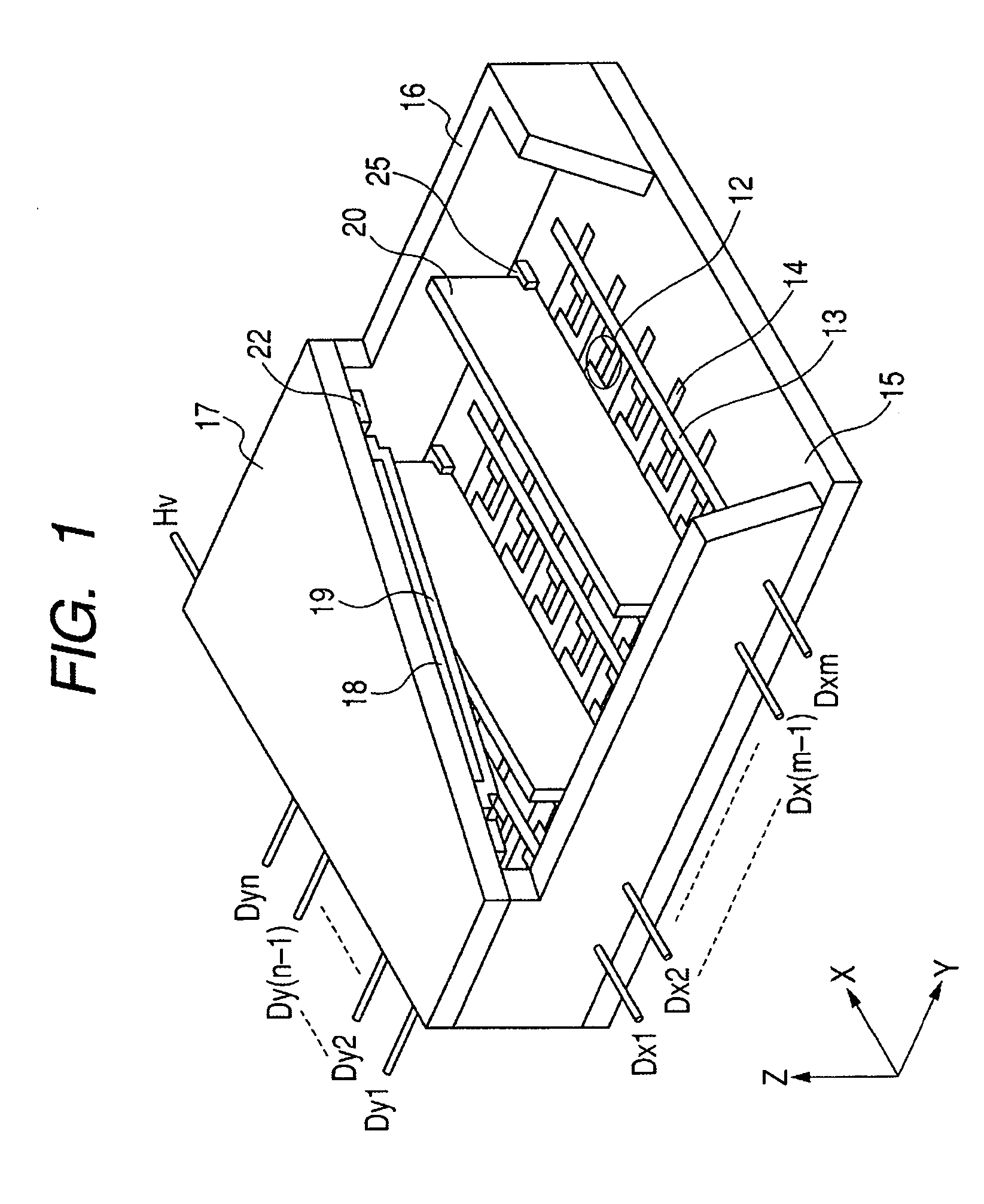
Image forming apparatus
a technology of forming apparatus and anode electrode, which is applied in the direction of discharge tubes, tubes with screens, instruments, etc., can solve the problems of low productivity, difficult to achieve secure contact of guard electrodes with spacers, and high electric field generation, and achieve satisfactory productivity.
- Summary
- Abstract
- Description
- Claims
- Application Information
AI Technical Summary
Benefits of technology
Problems solved by technology
Method used
Image

Examples
example 1
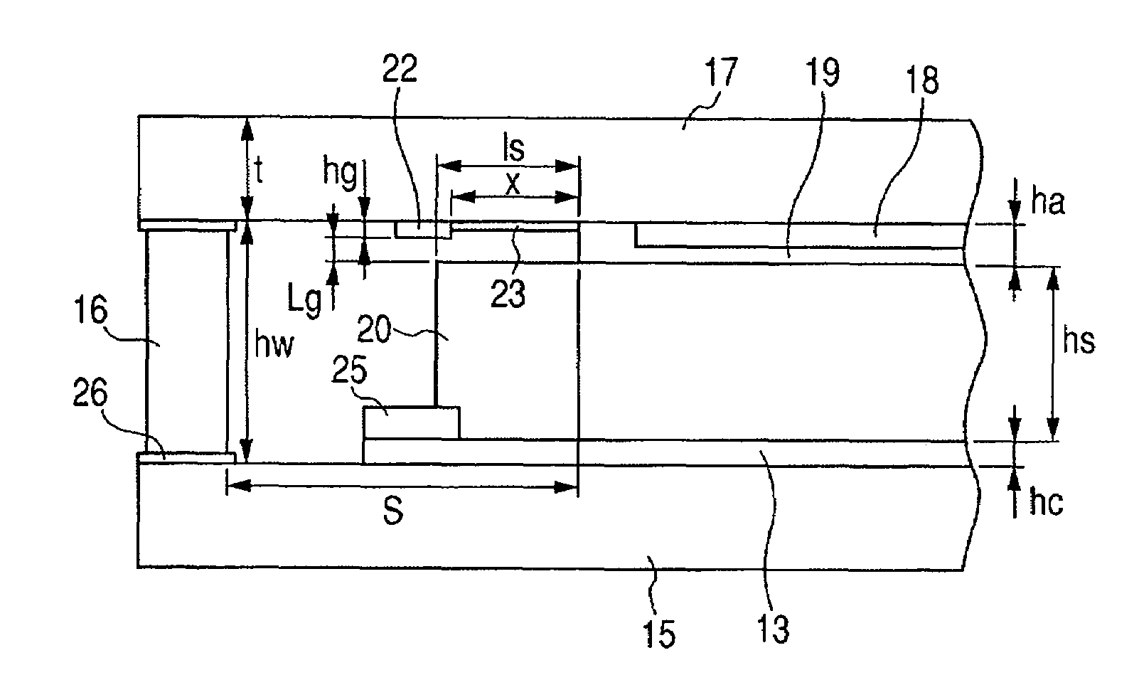
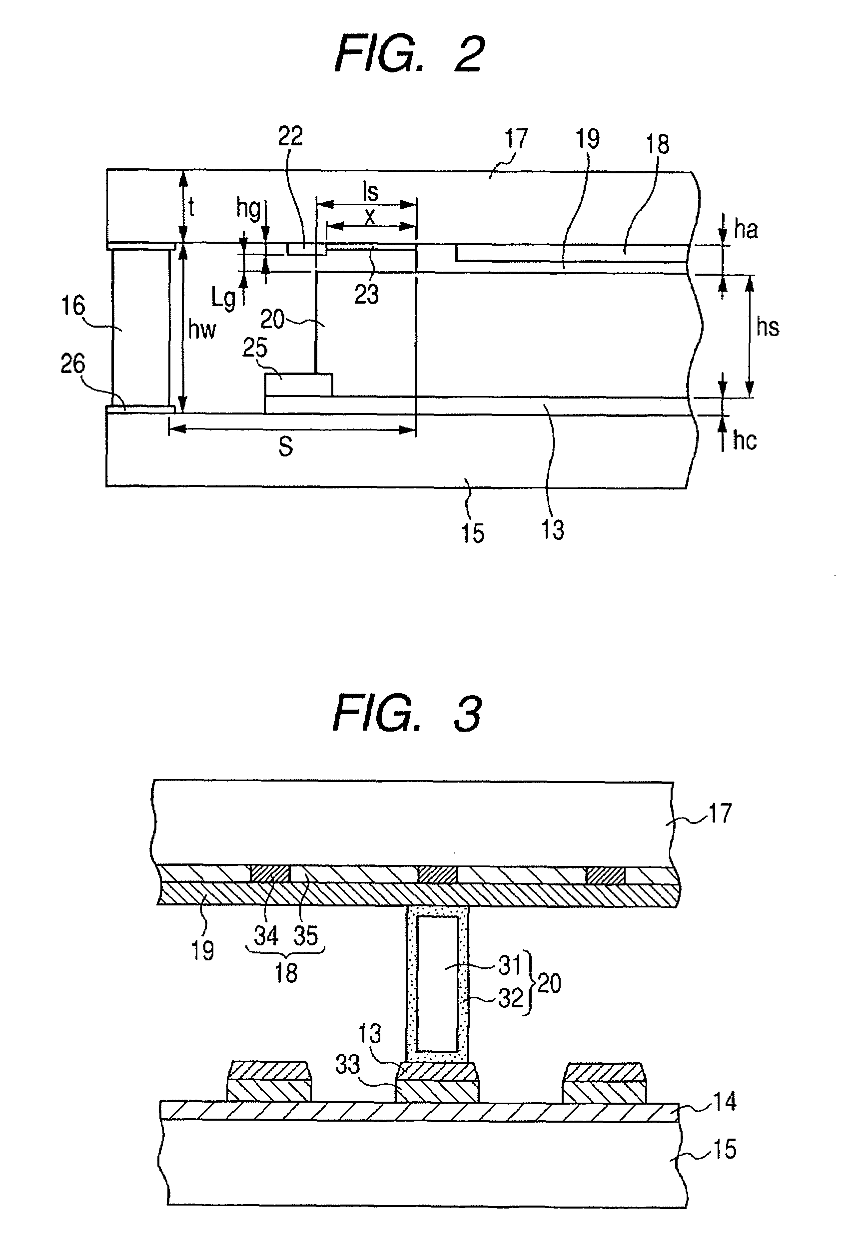
[0043]An image forming apparatus of a configuration shown in FIGS. 1 to 3 was constructed in the following manner.
[0044]As the substrate for the face plate 17, a high distortion point glass (PD200) of a thickness of 3 mm was employed. On such glass substrate, a guard electrode 22 was formed by printing a silver paste, and then a black conductor 34 was formed by printing. In apertures of the black conductor 34, phosphors 35 were formed by a screen printing. Then aluminum was vacuum evaporated thereon as a metal back 19. The thicknesses of the guard electrode, the black conductor and the metal back were determined in consideration of the dimensions of the components as follows. A spacer 20 was formed by sputtering, on a glass base member, a high resistance film 32 of WGeN with a thickness of about 100 nm. A frame member 16 was formed also by glass with a height of 3.6 mm. Between the frame member 16 and the rear plate 15, there was provided a frit glass layer 26 of a thickness of 220 ...
example 2
[0050]This example was different from the example 1 in that the distance between the frame member and the anode electrode was selected as 20 mm in order to obtain a compacter image display apparatus. Because of this change, the gap (Lg) between the guard electrode 22 and the spacer 20 was calculated as 10 μm from the equation (5). In this example, the portion of the spacer 20 opposed to the guard electrode 22 had a potential of about 1 kV and the row wiring was recessed by about 1 μm as in the example 1, so that the electric field strength between the guard electrode 22 and the spacer 20 was calculated as 1.1×10⁸ V / m.
[0051]Also in the image forming apparatus of the present example, no discharge was observed between the guard electrode 22 and the spacer 20.
example 3
[0052]This example was different from the example 1 in that the distance (S) between the metal back 19 and the frame member 16 was selected as 10 mm and the distance (x) between the metal back 19 and the guard electrode 22 was selected as 2 mm in order to obtain a further compacter image display apparatus, and in that the black conductor 34 was printed in two layers. This provides x≦0.5 hs, so that Lg≧7.5 μm is required from the equation (1), in order to apply Va =10 kV.
[0053]In the present example, the sealing operation was conducted by reducing the height of the gap regulating jig by 1 μm, in consideration of a fact that the row wiring was recessed by about 1 μm. More specifically, the gap regulating jig had a height of 4.029 mm. As a result, the height between the rear plate and the face plate in the vicinity of the frame member could be made same as that at the end of the metal back. In the present example, the black conductor 34 was selected as 20 μm and the metal back 19 was s...
PUM
 Abstract
Description
Claims
Application Information