
Semiconductor memory device comprising memory cells with floating gate electrode and method of production

a memory cell and semiconductor technology, applied in the direction of semiconductor devices, transistors, electrical devices, etc., can solve the problems of deterioration of transistor performance, no proportionality between current and channel width, and programming of floating gate memory cells, so as to improve the compatibility of lithography steps

Inactive Publication Date: 2007-07-31
POLARIS INNOVATIONS LTD
View PDF8 Cites 16 Cited by
  • Summary
  • Abstract
  • Description
  • Claims
  • Application Information

AI Technical Summary

Benefits of technology

[0008]In another aspect, the present invention provides a semiconductor memory device comprising memory cells with floating gate electrodes that avoids the occurrence of effects of a corner device and reduces short-channel effects, while at the same time ensuring data retention and endurance.
[0010]In still a further aspect, the present invention provides a semiconductor memory device comprising memory cells with floating gate electrodes that are endowed with an enlarged channel width and an improved uniformity of the distribution of the channel current.
[0016]Further preferred embodiments are provided with a recess in the substrate in the region of the memory cell array, in order to shift the cell transistors to a lower level and thereby improve the compatibility of the lithography steps that are common to the cell array and the periphery containing the address logic circuitry.

Problems solved by technology

Therefore, the devices show no proportionality between the current and the channel width.
The transistor performance is also deteriorated by the variation of the field strength across the channel.
A further disadvantage of this structure concerns the programming of the floating gate memory cells.
In these devices, the channel current increases approximately proportionally to the width of the channel, but the tunnel current of charge carriers passing across the tunnel oxide is restricted to a middle area of the channel, because the oxide layer in the marginal regions is too thick to be passed by tunneling charge carriers.
Therefore, it is not necessary to provide a large general oxide thickness in order to inhibit a premature oxide damage at the channel edges sustaining the main programming current flow, but the lateral restriction of the tunnel area effects the endurance of the device negatively.
This disadvantage originates from a higher current density during erase.
Unfortunately, a further scaling down or miniaturization of the memory cell requires the application of a thinner tunnel oxide, as the relation of the thickness of the tunnel oxide and the channel length must be kept constant, in order to cope with the short-channel effects.

Method used


Image

  • Semiconductor memory device comprising memory cells with floating gate electrode and method of production
  • Semiconductor memory device comprising memory cells with floating gate electrode and method of production
  • Semiconductor memory device comprising memory cells with floating gate electrode and method of production

Examples


Embodiment Construction

[0038]The making and using of the presently preferred embodiments are discussed in detail below. It should be appreciated, however, that the present invention provides many applicable inventive concepts that can be embodied in a wide variety of specific contexts. The specific embodiments discussed are merely illustrative of specific ways to make and use the invention, and do not limit the scope of the invention.

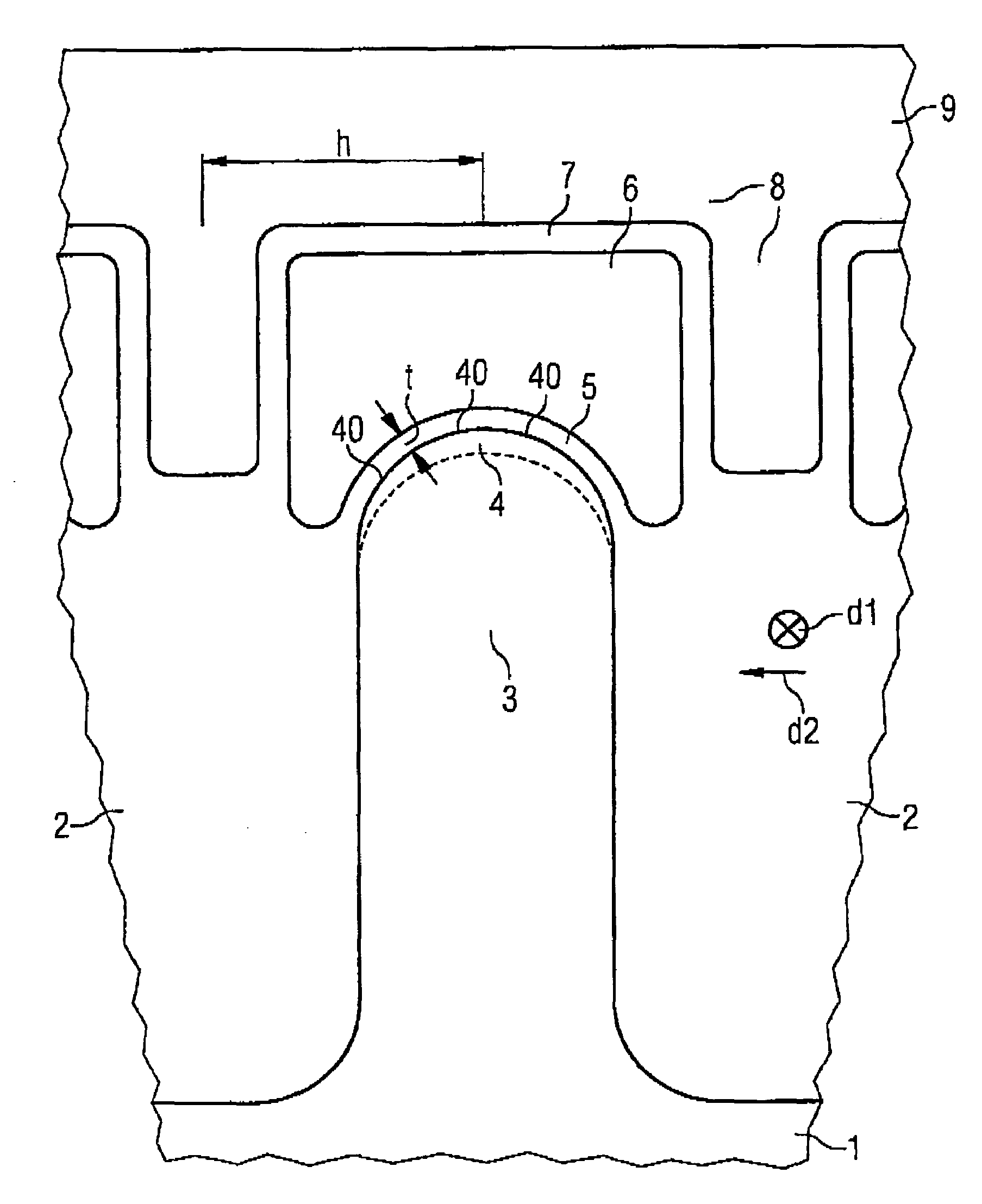
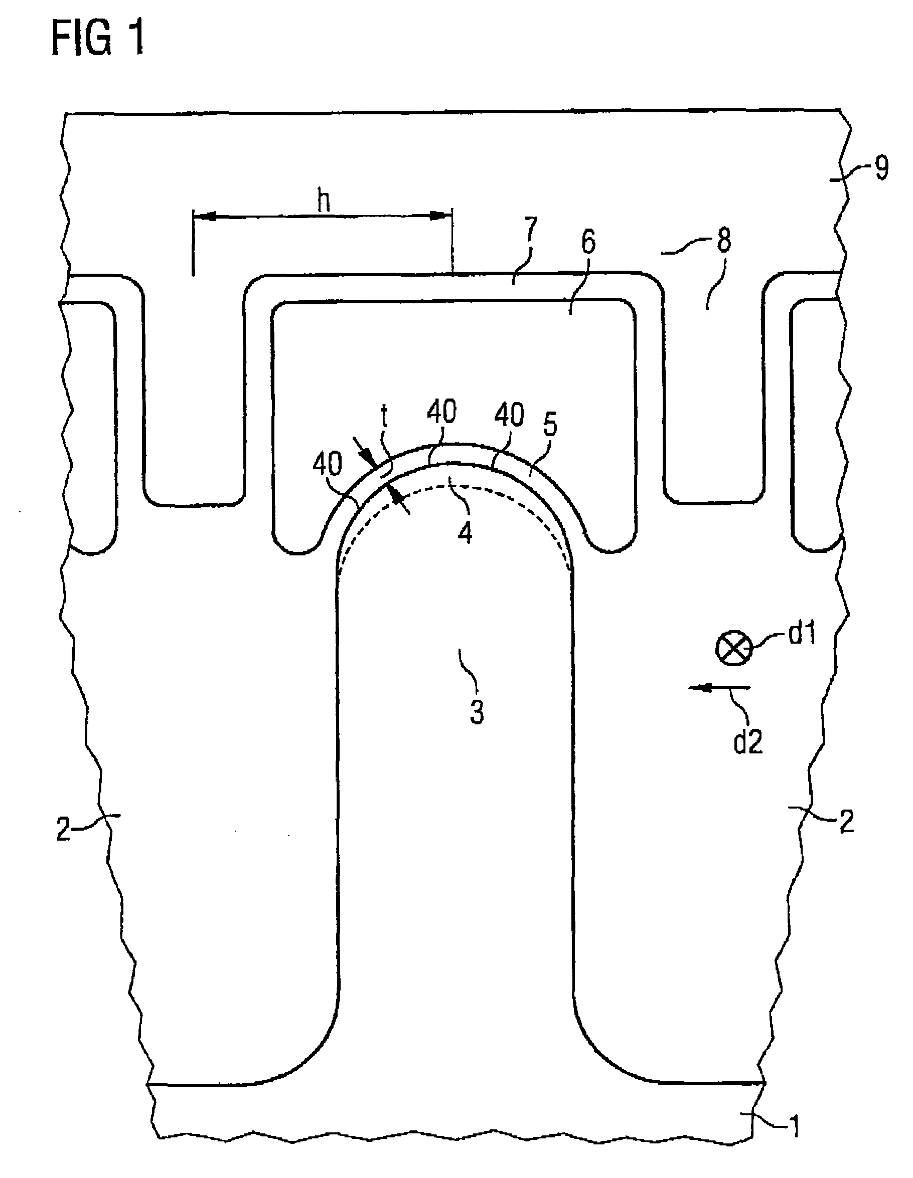
[0039]The floating gate memory cell comprises a channel that is curved along its width. This is accomplished by a curved upper surface of the transistor body that is located between shallow trench isolations. This upper surface is part of the active area. The thickness of the tunnel oxide varies at most slightly so that the lower surface of the floating gate electrode, which is arranged at a small distance above the transistor body, is adapted to the form of the upper surface of the transistor body. The curvatures are preferably concentric, at least in the primary tunnel area...


PUM


Abstract

Transistor bodies of semiconductor material located at a main surface of a semiconductor substrate between shallow trench isolations are provided with a rounded or curved upper surface. A floating gate electrode is arranged above said upper surface and electrically insulated from the semiconductor material by a tunnel dielectric having essentially the same tiny thickness throughout a primary tunnel area encompassing the area of curvature. The floating gate electrode may bridge the transistor body and is covered with a coupling dielectric provided for a control gate electrode, which forms part of a wordline.

Description

TECHNICAL FIELD[0001]The present invention concerns semiconductor memory devices with an array of memory cells, each of which is formed by a transistor structure comprising a channel that is located between source and drain and controlled by a gate electrode, and a floating gate electrode that is provided as storage means, like EEPROMs, NOR- and NAND-memories, and further concerns especially adapted methods of production of such devices.BACKGROUND[0002]NAND-memories are described in the publications of M. Ichige et al., “A novel self-aligned shallow trench isolation cell for 90 nm 4 Gbit NAND Flash EEPROMs” in 2003 Symposium on VLSI Technology Digest of Technical Papers, Session 7B-1; Y.-S. Yim et al., “70 nm NAND Flash Technology with 0.025 μm2 Cell Size for 4 Gb Flash Memory” in IEDM 2003, Session 34.1, 2003 IEEE Proceedings p. 819; D.-C. Kim et al., “A 2 Gb NAND Flash Memory with 0.044 μm2 Cell Size using 90 nm Flash Technology” in IEDM 2002, Session 37.1, 2002 IEEE Proceedings p...

Claims


Application Information

Patent Timeline
Patent Type & Authority Patents(United States)
IPC IPC(8): H01L27/108H01L29/76H01L29/94H01L31/062H01L31/119
CPCH01L21/28273H01L27/115H01L27/11521H01L29/51H01L29/66825H01L29/792H01L29/40114H10B69/00H10B41/30
Inventor KUSTERS, KARL-HEINZWILLER, JOSEFLIAW, CORVIN
Owner POLARIS INNOVATIONS LTD
Learn More