Semiconductor chip and display device using the same
a technology of semiconductor chips and display devices, applied in static indicating devices, instruments, non-linear optics, etc., can solve the problems of large drawing area of wirings from the terminals around the semiconductor chip, and large limitation of electrode arrangemen
- Summary
- Abstract
- Description
- Claims
- Application Information
AI Technical Summary
Benefits of technology
Problems solved by technology
Method used
Image
Examples
first embodiment
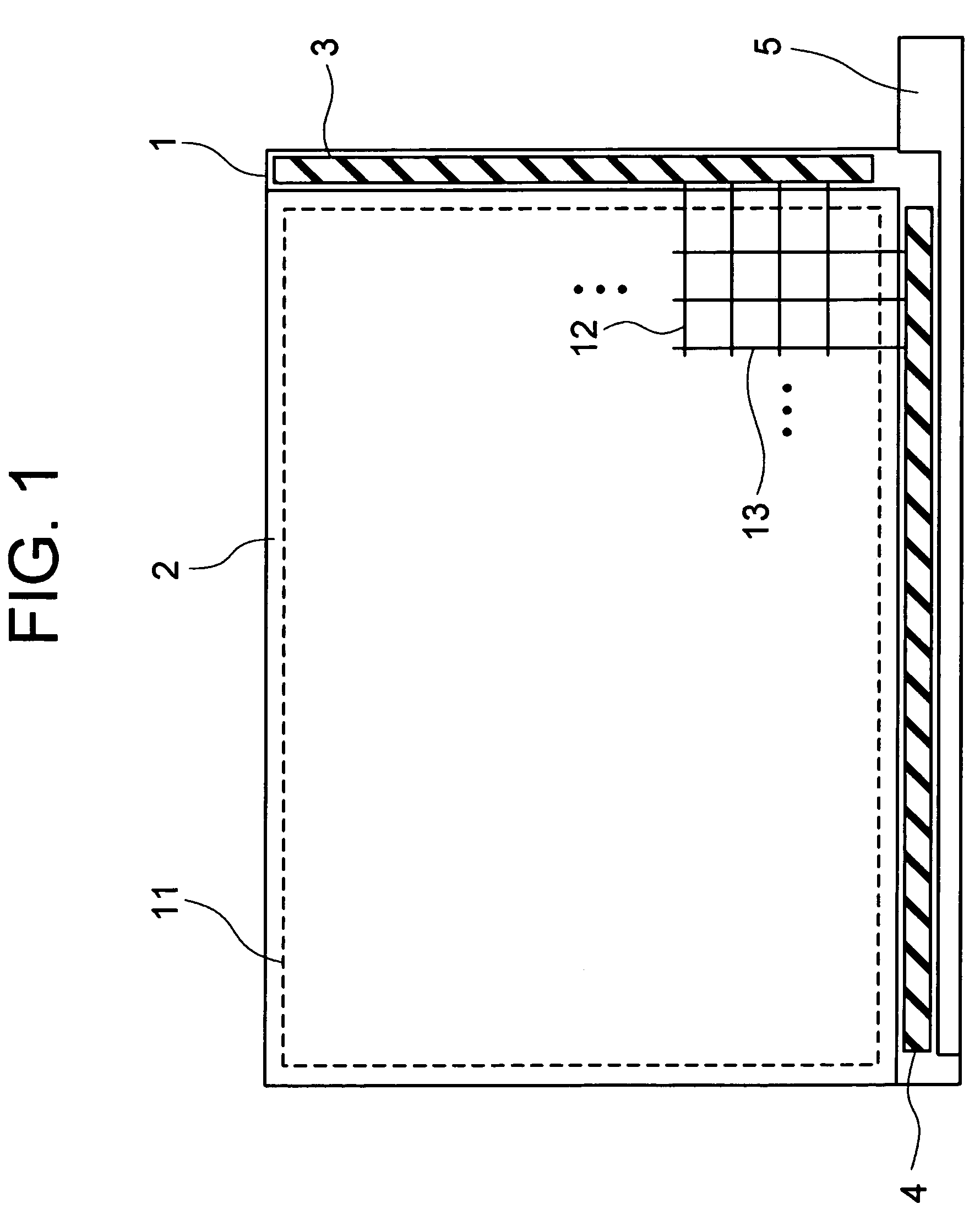
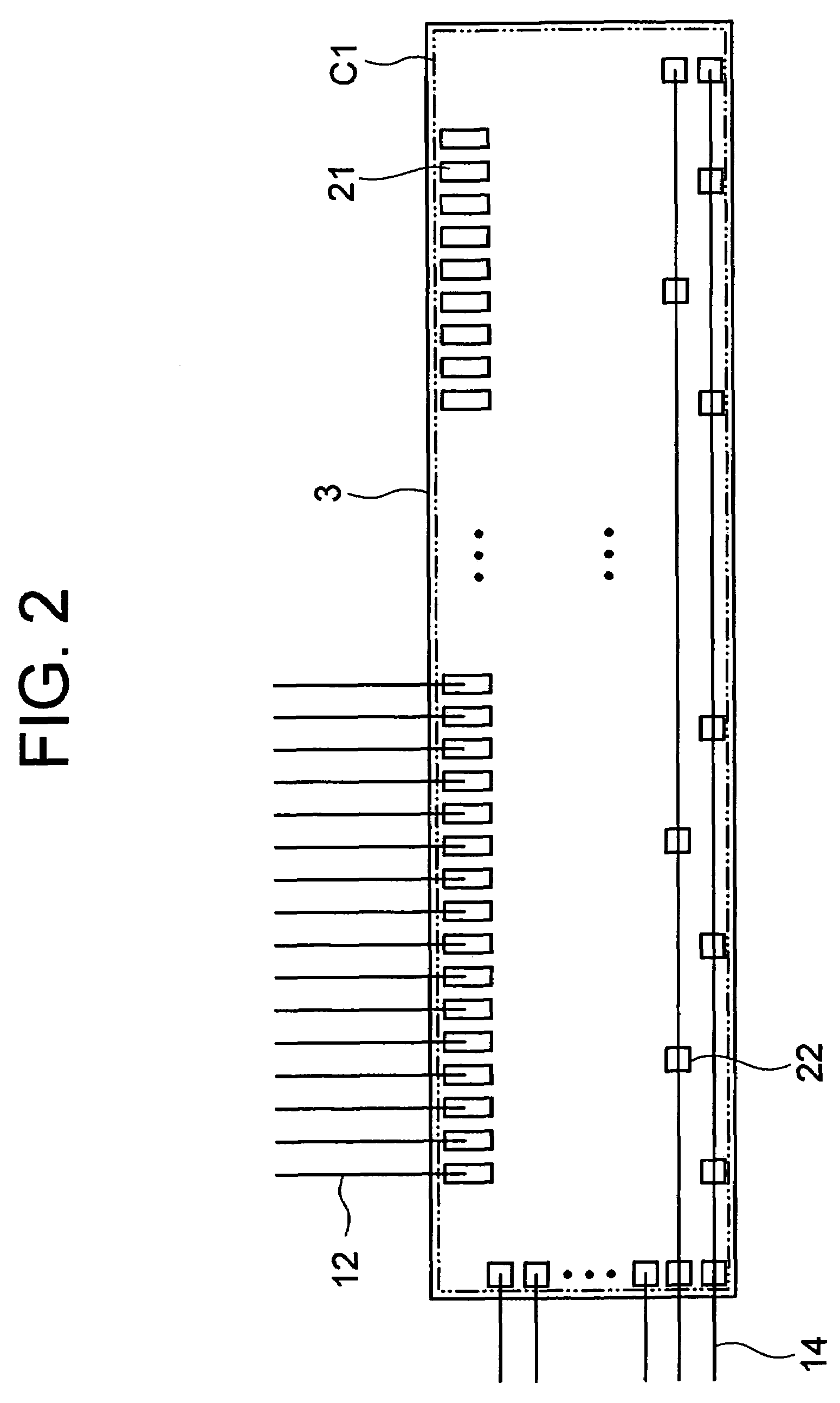
[0045]the present invention will be explained below by way of examples referring to a plan view of a liquid crystal display device shown in FIG. 1 and to the configurations of semiconductor chips shown in FIGS. 2 and 3.
[0046]In the liquid crystal display device shown in FIG. 1, a first substrate 1 and a transparent second substrate 2 are opposed to each other with a liquid crystal layer (not shown) interposed between them, and are bonded together with a sealant. As the first substrate 1 and the transparent second substrate 2, glass substrates are mainly used. Of course, plastic substrates may be used provided that a liquid crystal display device is realized.
[0047]The outer size of the first substrate 1 is larger than that of the transparent second substrate 2. In FIG. 1, the right edge and the lower edge of the first substrate 1 are projected from the second substrate 2, forming a frame part on which semiconductor chips are mounted. On the frame part, semiconductor chips 3 and 4, ma...
sixth embodiment
[0103]FIG. 15 is plan view of a liquid crystal display device of the present invention, and FIG. 16 is a plan view of the semiconductor chip 4 for driving signal lines shown in FIG. 15, showing the connecting relationship with the wirings.
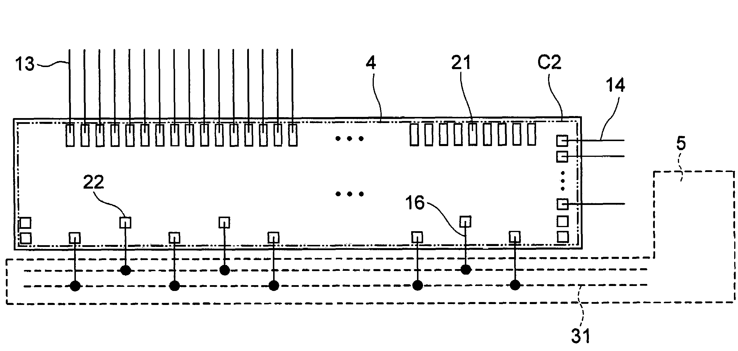
[0104]The aspect different from FIG. 13 showing the fifth embodiment is as follows. That is, the flexible wirings 31, corresponding to the control / power supply lines 14, are formed on the flexible wiring board 5B mounted on the frame of the display unit 11. The semiconductor chip 4 is mounted on the flexible wiring board 5B, and the output terminals 21 of the semiconductor chip 4 are connected with the signal lines 13 of the display unit 11, respectively. Further, the connecting terminals 22 of the semiconductor chip 4 are connected with the flexible wirings 31. The connecting terminals 22 arranged on the short edge side of the semiconductor chip 5 are connected with the control / power supply lines 14 formed on the substrate 1. The control / power sup...
PUM
| Property | Measurement | Unit |
|---|---|---|
| voltage | aaaaa | aaaaa |
| length | aaaaa | aaaaa |
| width | aaaaa | aaaaa |
Abstract
Description
Claims
Application Information


