Data form converter between serial and parallel

Active Publication Date: 2007-08-07
RENESAS ELECTRONICS CORP
View PDF18 Cites 25 Cited by
  • Summary
  • Abstract
  • Description
  • Claims
  • Application Information

AI Technical Summary

Benefits of technology

[0019]As described above, according to the present invention, a serial-to-parallel or parallel-to-serial conversion section operates according to an input clock and a single frequency-divided clock that is generated from the input clock by a frequency-dividing section with a variable frequency-division ratio. Accordingly, by designing a single serial-to-parallel or parallel-to-serial conversion section, a serial-to-parallel or parallel-to-serial conversion can be performed for different numbers of bits of parallel data. Therefore, it is not necessary to design different serial-to-parallel or parallel-to-serial converters for every number of bits of parallel data, thus largely reducing the design workload.
[0020]Moreover, since the serial-to-parallel or parallel-to-serial converter according to the present invention can be structured to operate according to only the input clock and the frequency-divided clock, the circuit structure is made simple and thereby the circuit design is made easier.
[0022]Furthermore, according to another embodiment of the invention, the serial-to-parallel or parallel-to-serial converter can be arranged in multiple stages. Thus, even in a case of forming a high-speed data form converter, it is enough that a part of that circuit is design to perform a high-speed operation. This reduces the cost of the entire circuit and also makes it easier to increase the operation speed of the circuit. In addition, such multi-stage circuit allows a plurality of circuit components having the same circuit structure to be used, resulting in reduction of the design workload and design time.

Problems solved by technology

However, a difference between an operating speed in an LSI and the signal transmission rate between LSIs is large.
Such a conventional serial-parallel converter, however, cannot convert serial data to parallel data at a ratio other than the ratio of 1:2n.
For example, at a position where data transfer occurs over different frequency-divided clocks, setup and hold time of the first and second flip-flop circuits may become severe.
This makes it more difficult to design the serial-parallel converter.
Thus, this parallel-serial converter also has a problem that the number of bits of low-speed parallel data to be converted into serial data is uniquely determined by the frequency-frequency-division ratio of the frequency divider.
As a result, in order to perform parallel-serial conversion at two different ratios, for example, 4:1 and 5:1, two kinds of parallel-serial converters corresponding to those ratios, respectively, have to be designed, thus increasing design workload.

Method used


Image

  • Data form converter between serial and parallel
  • Data form converter between serial and parallel
  • Data form converter between serial and parallel

Examples


first embodiment

1. First Embodiment

[0046]1.1) Circuit Structure

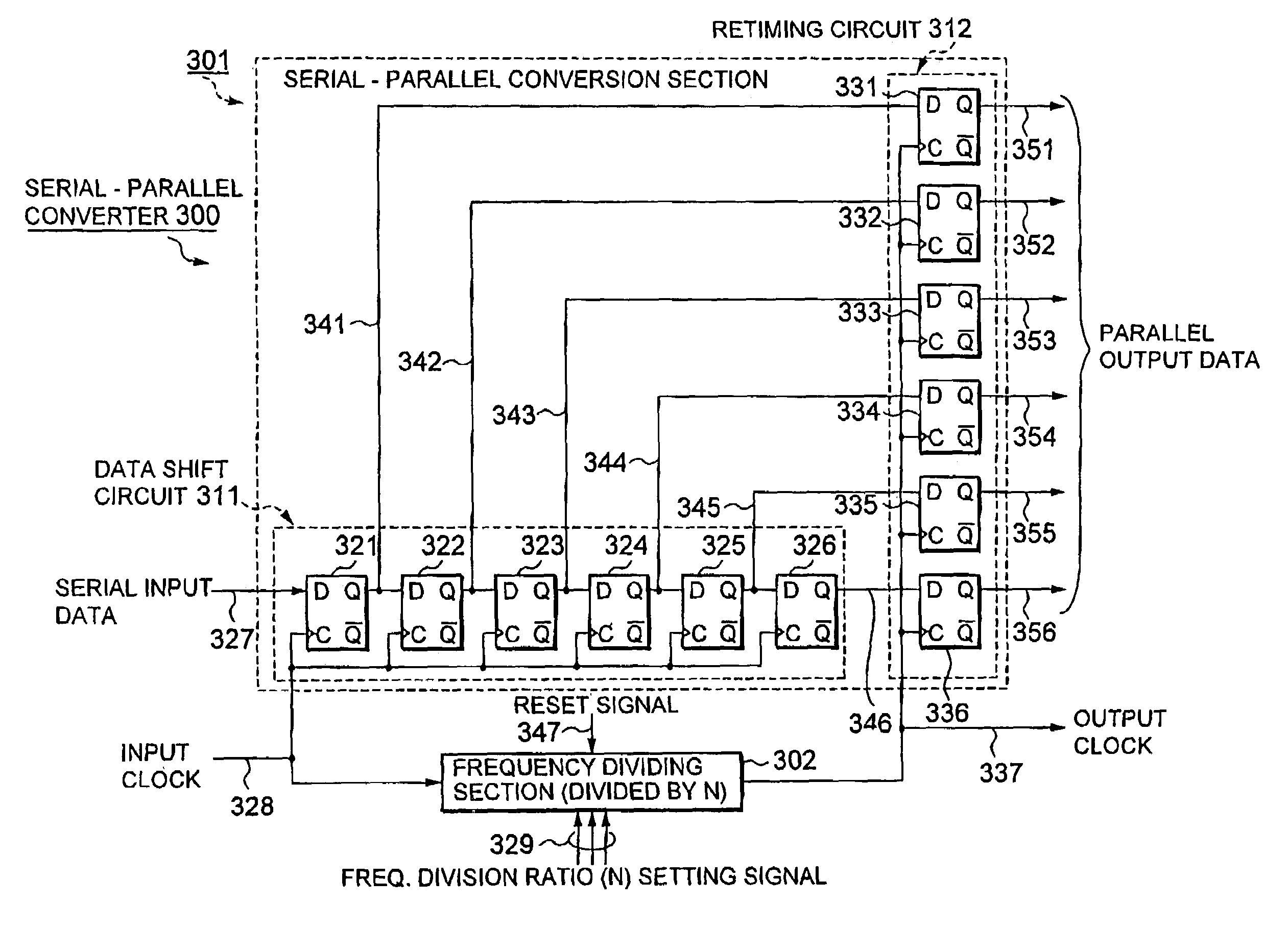
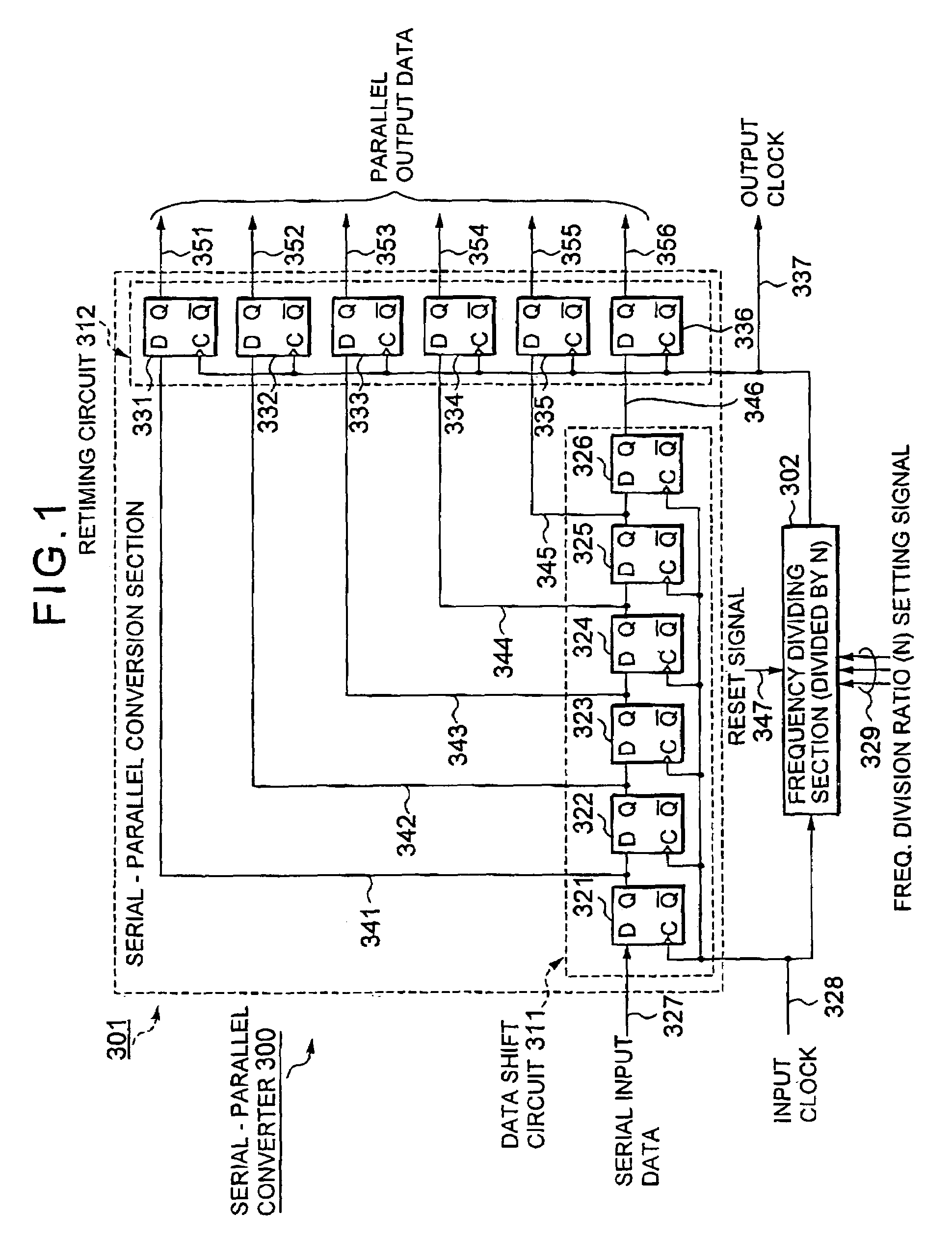
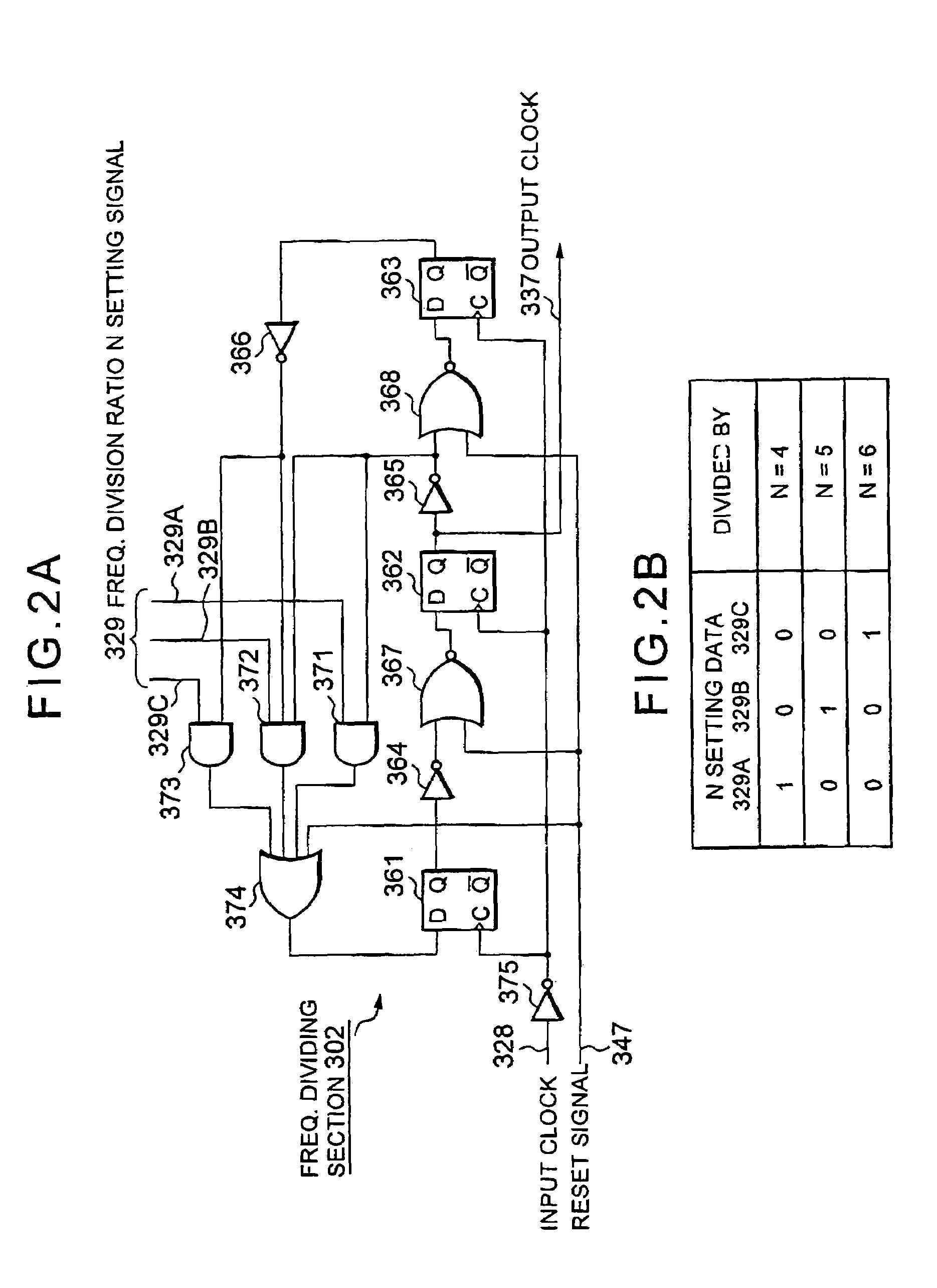
[0047]Referring to FIG. 1, a serial-parallel converter 300 according to a first embodiment of the present invention includes a serial-parallel conversion section 301 and a frequency dividing section 302. The serial-parallel conversion section 301 is comprised of a data shift circuit 311 and a retiming circuit 312. The data shift circuit 311 includes first to sixth flip-flop circuits 321–326 that are connected in a cascade connection, and sequentially shifts serial input data 327 received at a data input terminal D of the first flip-flop circuit 321 according to an input clock 328. The input clock 328 is also supplied to the frequency dividing section 302. A frequency-division ratio of the frequency dividing section 302 can be set to a selected one (N) of various frequency-division ratios depending on a frequency-division ratio setting signal 329.

[0048]The retiming circuit 312 includes first to sixth flip-flop circuits 331–336, each of w...

second embodiment

2. Second Embodiment

[0081]2.1) Circuit Structure

[0082]Referring to FIG. 10, a serial-parallel converter 400 according to a second embodiment of the present invention includes a 1:2 serial-parallel conversion section 401, a first serial-parallel conversion section 411, a second serial-parallel conversion section 412, and a frequency dividing section 413. Each of the serial-parallel conversion sections 411 and 412 has the same circuit structure as that of the serial-parallel conversion section 301 as shown in FIG. 1. Accordingly, the data shift circuit 311 and the retiming circuit 312 are depicted by dashed lines in each of the serial-parallel conversion sections 411 and 412. The frequency dividing section 413 also has the same circuit structure as that of the frequency dividing section 302 as shown in FIG. 1.

[0083]In such a circuit as shown in FIG. 10, the input data 327 and the input clock 328 are first input to the 1:2 serial-parallel conversion section 401. The 1:2 serial-parallel...

third embodiment

3. Third Embodiment

[0099]3.1) Outline of Circuit

[0100]Referring to FIG. 13, a parallel-serial converter 500 according to a third embodiment of the present invention includes a parallel-serial conversion section 501 and a frequency dividing section 502. As the frequency dividing section 502, the frequency dividing section 302 or 302A shown in FIG. 2 or 3 in the first example may be used. An input clock 503 is supplied to both the frequency dividing section 502 and the parallel-serial conversion section 501. When a reset signal 504, which corresponds to the reset signal 347 in FIG. 1, is changed from “1” to “0,” the frequency dividing section 502 starts frequency division of the input clock 503 (see the input clock. 328 shown in FIGS. 4(b), 5(b), and 6(b)), thereby outputting a frequency-divided clock 505 (corresponding to the output clock 337 of the first example shown in FIGS. 4(d), 5(d), and 6(d)). The frequency-divided clock 505 is then supplied to the parallel-serial conversion s...


PUM


Abstract

A data form converter allowing parallel-to-serial or serial-to-parallel conversion at various conversion ratios is disclosed. A frequency divider divides an input clock in frequency at a variable frequency division ratio to produce a single frequency-divided clock. A data shift circuit shifts serial input data according to the input clock to output n-bit parallel data, where n is determined depending on the variable frequency division ratio. A retiring section synchronizes the n-bit parallel data with the single frequency-divided clock to output parallel output data.

Description

BACKGROUND OF THE INVENTION[0001]1. Field of the Invention[0002]The present invention relates to a data form converter, which converts data form from serial to parallel or from parallel to serial.[0003]2. Description of the Related Art[0004]LSI (Large Scale Integration) technology has been remarkably developed, so that an operating clock in an LSI has been increased to several hundred megahertz (MHz) and a signal transmission rate between LSIs has been increased to several gigabits per second (Gbps). However, a difference between an operating speed in an LSI and the signal transmission rate between LSIs is large. In order to allow an LSI to output / input data to / from outside, a parallel-to-serial (hereinafter, denoted by “parallel-serial”) converter may be provided at an output stage of the LSI so as to convert low-speed parallel data in the LSI into high-speed serial data, allowing the high-speed serial data to be output from the LSI to the outside. Moreover, by providing a serial-t...

Claims


Application Information

Patent Timeline
IPC IPC(8): H03M9/00
CPCH03M9/00C02F1/484C02F2201/483
Inventor TAKEUCHI, MASAHIROSAEKI, TAKANORITANAKA, KENICHI
Owner RENESAS ELECTRONICS CORP
Why Eureka
Try Eureka