Side emitting LED and lens

a technology of led and side-emitting diodes, which is applied in the direction of instruments, lighting and heating apparatus, semiconductor devices for light sources, etc., can solve the problems of inability to perform, ineffective distance can be shortened, and ineffective distance can be reduced, so as to reduce the overlap of optical paths, prevent improper reflection or refraction, and reduce the stress concentration during fabrication

Inactive Publication Date: 2007-08-07
CORETRONIC
View PDF3 Cites 93 Cited by
  • Summary
  • Abstract
  • Description
  • Claims
  • Application Information

AI Technical Summary

Benefits of technology

[0008]Therefore one object of the present invention is to provide a side emitting LED lens that reduces “optical path overlap” on boundaries of two light paths to prevent an imprope

Problems solved by technology

There is an ineffective distance L1 where mixing cannot be performed.
However, if the lighting profile of the individual LEDs is flattened, the ineffective distance can be shortened.
1. As the light is divided into two optical paths, an “optical path overlap” easily occurs on boundaries of the two optical paths. As a result, an improper reflection or refraction takes place. Referring to FIG. 4, there is an optical path overlap zone α between the first refractive surface 12 and the second refractive surface 13. If the ligh

Method used


Image

  • Side emitting LED and lens
  • Side emitting LED and lens
  • Side emitting LED and lens

Examples


Embodiment Construction

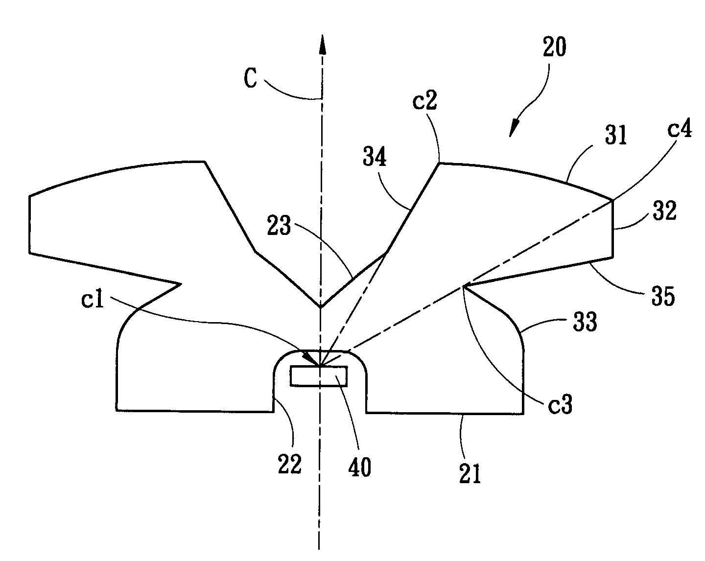
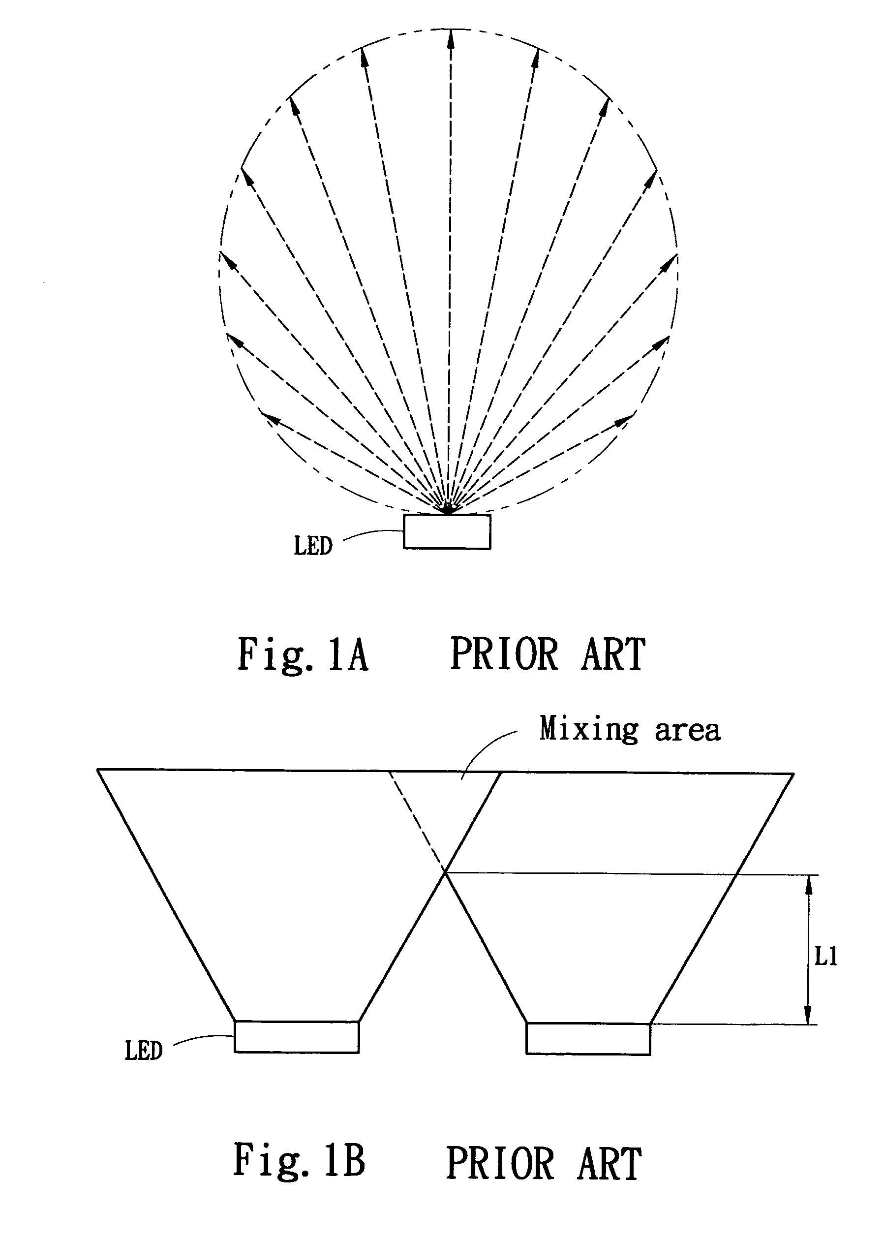
[0022]Please refer to FIG. 5 showing a side emitting light emitting diode (LED) of an embodiment of the present invention. The side emitting LED includes a lens 20 and a light source. The lens 20 of the embodiment includes a bottom surface 21, an incident surface 22, a reflective surface 23, a first refractive surface 31, a second refractive surface 32, a third refractive surface 33, a first transitive surface 34 and a second transitive surface 35. The lens 20 is a package structure for the light source, such as semiconductor lighting element. The semiconductor lighting element includes a LED chip 40 (as shown in FIG. 6). In the embodiment, a light emitted from the LED chip 40 is presented according to a Lambertion energy distribution (shown in FIG. 1A).

[0023]In the embodiment, the incident surface 22 is connected to the bottom surface 21 and surrounds the LED chip 40. The reflective surface 23 is surrounding and abutting to a central optic axis C of the lens 20 and forms an angle w...


PUM


Abstract

A lens of a side emitting LED includes a bottom surface, an incident surface, a reflective surface, a first refractive surface, a second refractive surface and a third refractive surface. An light emitted by a LED enters the lens through the incident surface. A portion of the light is reflected by the reflective surface in an internal total reflection manner to the second refractive surface and emits out of the lens along a first optical path. The other portion of light directly emits out of the lens through the first refractive surface and the third refractive surface. A transitive surface is located between the first refractive surface and the reflective surface. Such a design allows the light entered the lens through the incident surface not cross with the transitive surface. Hence an improper reflection or refraction can be prevented.

Description

FIELD OF THE INVENTION[0001]The present invention relates to a side emitting light emitting diode (LED) and particularly to a lens of a side emitting LED.BACKGROUND OF THE INVENTION[0002]In general, a light emission of a conventional light emitting diode (LED) is that the light emission path is normal to the light emission surface of the LED chip, and a Lambertion energy distribution fashion is presented (referring to FIG. 1A). For applications in traffic lights, illumination or other indicative signals, due to the limitation of energy distribution profile, if a plurality of LEDs are mixed optically (such as mixing of light intensity, color lights, or the like), a desired mixing result is obtained only at a selected distance from the light emission surface of the LEDs (referring to FIG. 1B). There is an ineffective distance L1 where mixing cannot be performed. However, if the lighting profile of the individual LEDs is flattened, the ineffective distance can be shortened.[0003]Lumile...

Claims


Application Information

Patent Timeline
IPC IPC(8): G02B6/10F21V5/00
CPCF21V5/04F21V7/0091G02B19/0071G02B19/0028G02B19/0061F21Y2101/02H01L33/58H01L33/60F21Y2115/10
Inventor CHOU, WEN-BINSHIAU, TZENG-KEHOU, TENG-CHAO
Owner CORETRONIC
Why Eureka
Try Eureka