Testing for operating life of a memory device with address cycling using a gray code sequence

a memory device and address cycling technology, applied in the field of memory device testing, can solve the problems of affecting the results of such testing, affecting the test system, and faulty characteristics, and achieve the effect of minimizing the failure rate of the charge gain

Inactive Publication Date: 2007-08-07
MONTEREY RES LLC
View PDF15 Cites 26 Cited by
  • Summary
  • Abstract
  • Description
  • Claims
  • Application Information

AI Technical Summary

Benefits of technology

[0015]Accordingly, in a general aspect of the present invention, failure of a flash memory cell after a last row of an array of flash memory cells is accessed is determined to be from charge gain failure when a la...

Problems solved by technology

Any deleterious effect on the results of such testing from faulty characteristics of the test s...

Method used


Image

  • Testing for operating life of a memory device with address cycling using a gray code sequence
  • Testing for operating life of a memory device with address cycling using a gray code sequence
  • Testing for operating life of a memory device with address cycling using a gray code sequence

Examples


Embodiment Construction

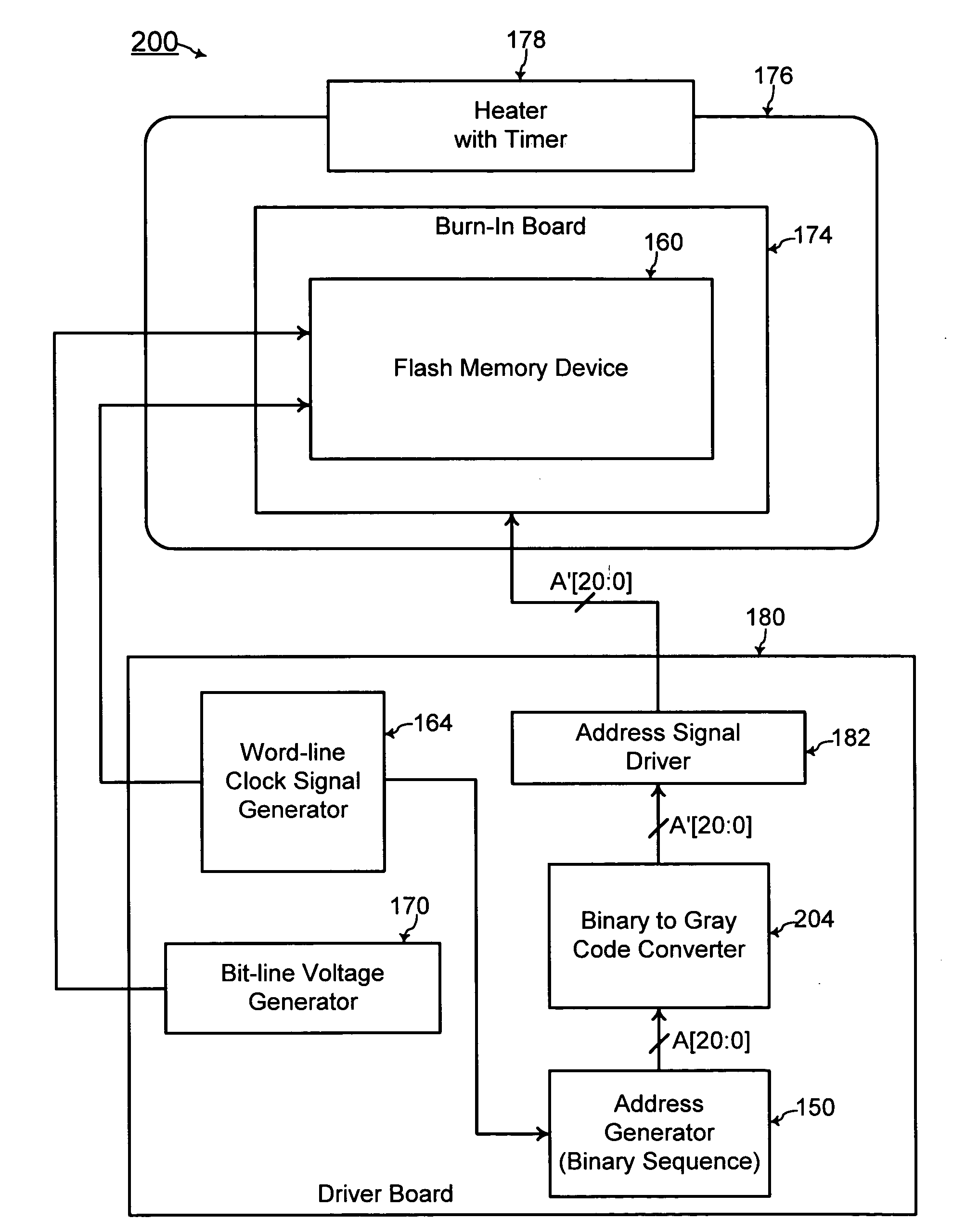
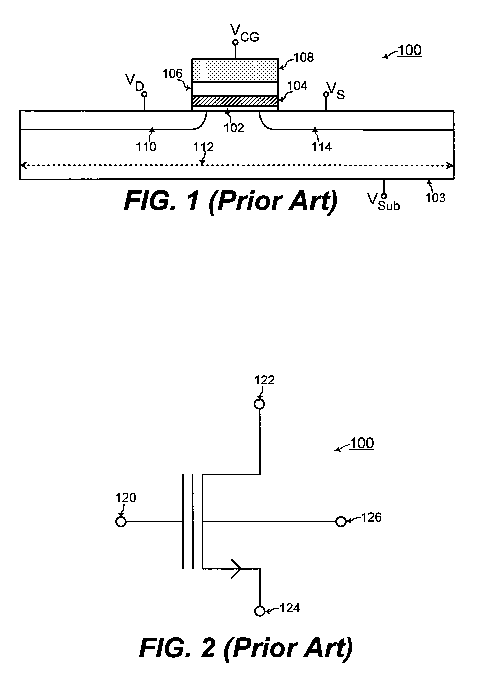
[0037]FIG. 6 illustrates components of a flash memory device 160 including the array of flash memory cells 152. Components considered part of the flash memory device 160 are outlined in solid lines in FIG. 6, and components not considered part of the flash memory device 160 are outlined in dashed lines in FIG. 6. FIG. 6 includes components (outlined in dashed lines) that are not part of the flash memory device 160 and are for performing HTOL (high temperature operating life) stressing for the flash memory device 160.

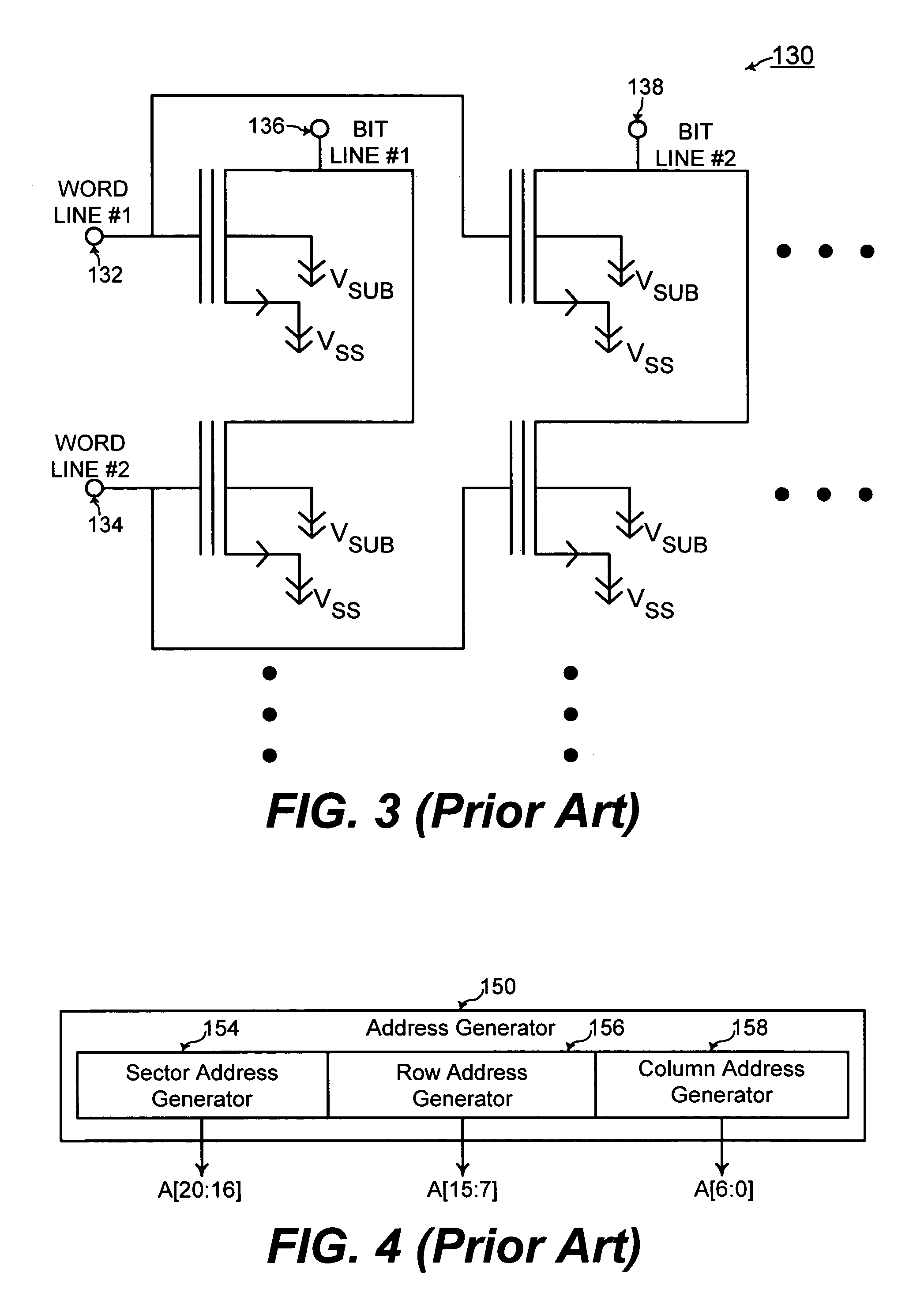
[0038]The flash memory device 160 includes an X-decoder 162 that inputs and decodes the row address A[15:7] to couple a clock signal from a word line clock signal generator 164 to the word line for a selected one of the five hundred twelve rows as specified by the row address A[15:7]. For example, the clock signal from the clock signal generator 164 is a 1 MHz (mega-hertz) typical clock signal wave-form. In addition, the flash memory device 160 includes sector switches 1...


PUM


Abstract

In a method and system for cycling through addresses of a memory device, a respective bit pattern comprised of a predetermined number of bits is generated for each address. The respective bit pattern for each of the addresses is cycled through with a transition of less than the predetermined number of bits for sequencing to each subsequent address. For example, the respective bit pattern for each of the addresses is cycled through in a gray code sequence. By limiting the number of transitions in the address bits, charge gain failure of a flash memory device is minimized and even may be eliminated.

Description

TECHNICAL FIELD[0001]The present invention relates generally to testing of memory devices, and more particularly, to cycling through addresses of a flash memory device with minimized charge gain failure during testing of the flash memory device.BACKGROUND OF THE INVENTION[0002]Referring to FIG. 1, a flash memory cell 100 of a flash memory device includes a tunnel dielectric structure 102 typically comprised of silicon dioxide (SiO2) or nitrided oxide as known to one of ordinary skill in the art of integrated circuit fabrication. The tunnel dielectric structure 102 is disposed on a semiconductor substrate or a p-well 103. In addition, a floating gate structure 104, comprised of a conductive material such as polysilicon for example, is disposed over the tunnel dielectric structure 102. A dielectric structure 106, typically comprised of silicon dioxide (SiO2), is disposed over the floating gate structure 104. A control gate structure 108, comprised of a conductive material, is disposed...

Claims


Application Information

Patent Timeline
IPC IPC(8): G06F12/00
CPCG11C16/04G11C29/50
Inventor TEOH, WAN YENLAW, CHE SEONG
Owner MONTEREY RES LLC
Why Eureka
Try Eureka