Image sensors with distributed amplifiers and related methods

a technology of image sensors and amplifiers, applied in the field of image sensors with distributed amplifiers, can solve the problems of compromising the noise level achievable, introducing noise to the detected image, and the noise of the readout chain

Active Publication Date: 2007-09-04
STMICROELECTRONICS (RES & DEV) LTD
View PDF14 Cites 25 Cited by
  • Summary
  • Abstract
  • Description
  • Claims
  • Application Information

AI Technical Summary

Problems solved by technology

Each of these components introduces noise to the detected image.
However, each component of the readout chain introduces noise to the process.
The-pixel transistors must be small to achieve a small pixel size and high fill factor and this compromises the noise level achievable.
This noise source is often dominant over the remaining circuit noise.
Often some means of removing amplifier column offsets is applied (auto-zero or feedback) which tends to increase this noise.
Excessive noise degrades the performance of an image sensor, while an excessively large circuit will limit the applications to which the image sensor can be put or be commercially unattractive.

Method used


Image

  • Image sensors with distributed amplifiers and related methods
  • Image sensors with distributed amplifiers and related methods
  • Image sensors with distributed amplifiers and related methods

Examples


Embodiment Construction

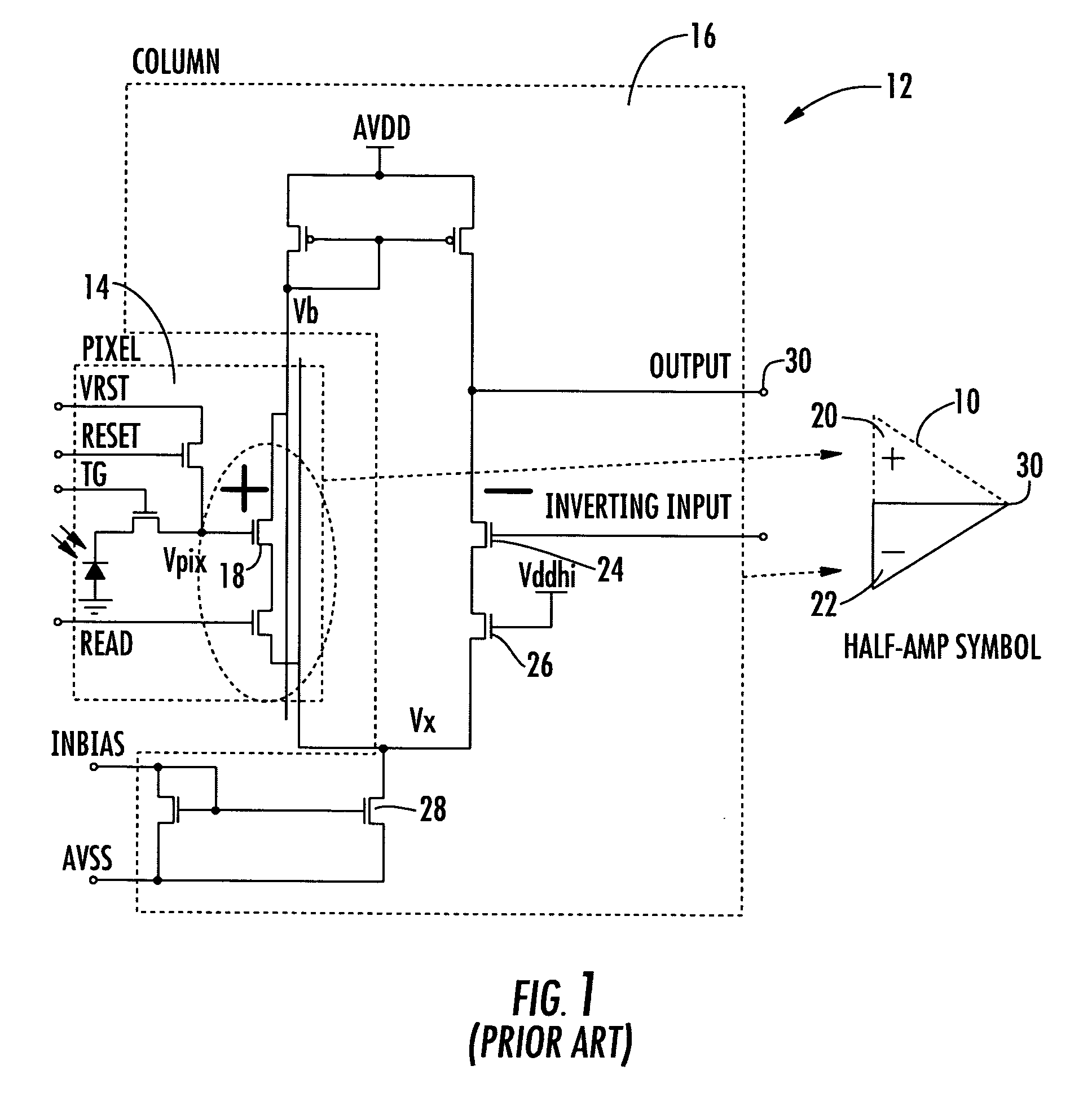
[0025]A known “distributed amplifier”10 is shown in FIG. 1, the architecture of which is shown generally at 12. Such distributed amplifiers are known, for example from U.S. Pat. No. 6,130,423 assigned to Pixel Cam Inc., and U.S. Pat. No. 6,084,229 assigned to Photon Vision Systems LLC. Distributed amplifiers are currently used to linearize a pixel source follower and / or to attenuate reset noise of a three transistor pixel.

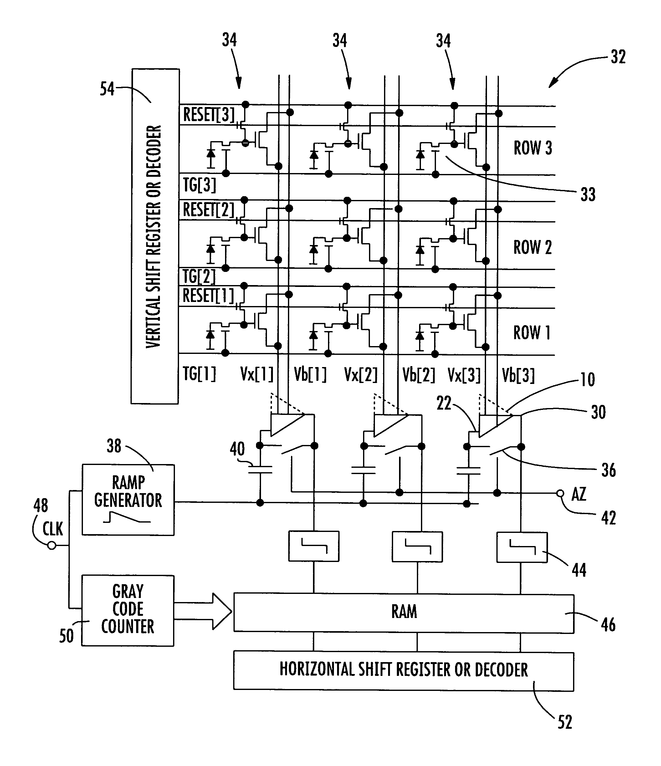
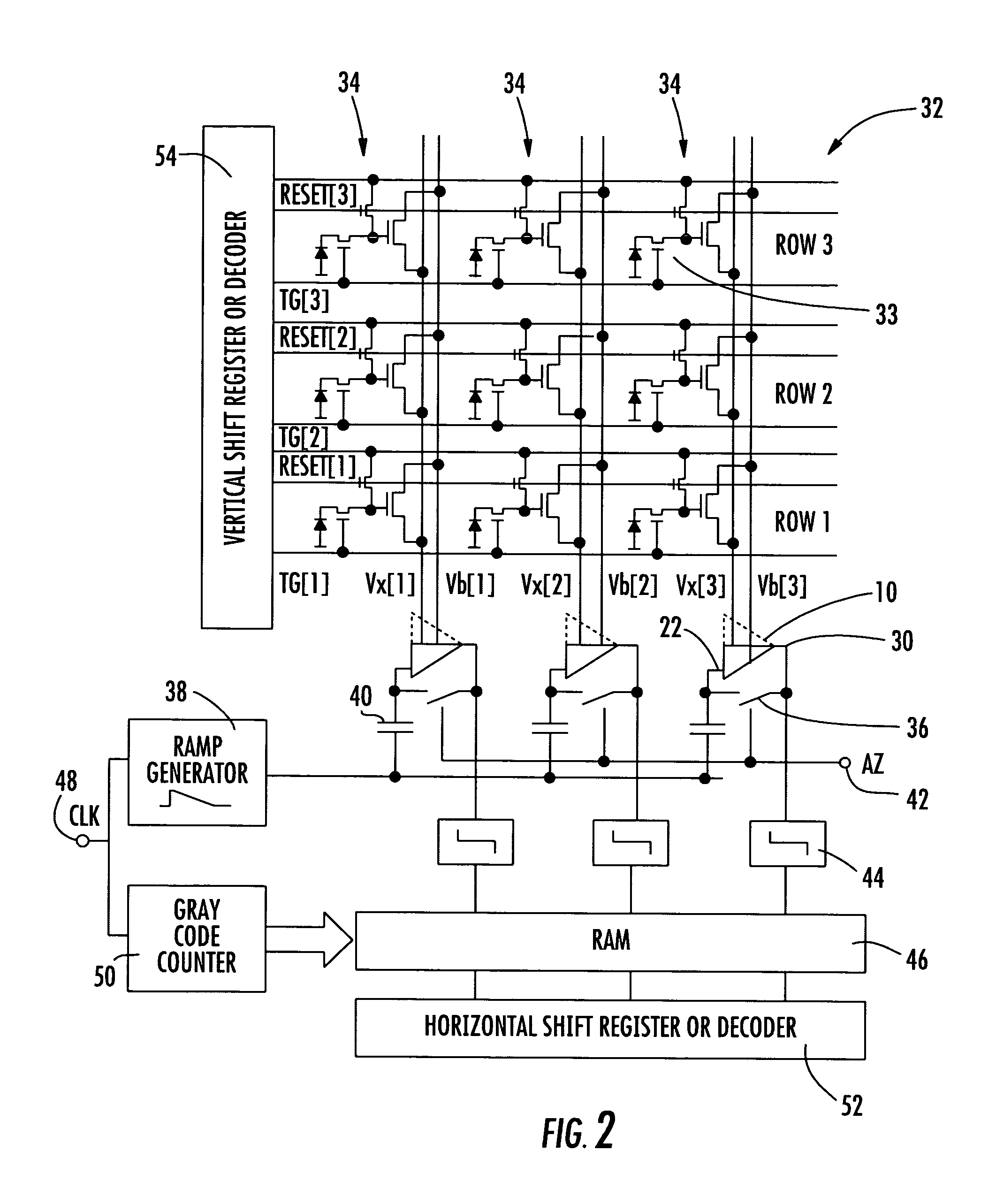
[0026]The present invention provides an image sensor in which all the components of the readout chain, that is the source follower (present for all active pixels), a sampling circuit, a preamplifier, and an analog to digital conversion circuit, are combined in one single circuit. In this circuit, the functions of these components can be described as being integrated. In particular, a distributed amplifier is provided which is integrated with an ADC for noise reduction. This is achieved by using a pixel amplifier as a column comparator.

[0027]The present invention pe...


PUM


Abstract

The image sensor makes use of a distributed amplifier having its non-inverting input provided by a pixel amplifier transistor, and its inverting input and output provided in the pixel's column circuitry. The distributed amplifier is directly integrated with the image sensor's ADC circuit, and sampling and autozero are performed in a single step, thus reducing the number of noise contributions made by the components of the image sensor's readout chain.

Description

FIELD OF THE INVENTION [0001]According to a second aspect of the present invention, there is provided an integrated circuit comprising an image sensor which comprises pixel circuitry, readout circuitry and a distributed amplifier which comprises a first input residing in the pixel circuitry, and a second input and output residing in the readout circuitry, and wherein the second input is coupled to a ramp voltage generator and the output is coupled to an analog to digital converter (ADC) or conversion means. A switch or switch means is provided between the output and second input, and is selectively operable by an autozero signal. Features of the first aspect may also be applied to the second aspect.BACKGROUND OF THE INVENTION [0002]A typical solid-state image sensor comprises a light gathering stage and a readout chain. An example of such a sensor is described in S. K. Mendis, S. E. Kemeny, R. C. Gee, B. Pain, C. O. Staller, Q. Kim, E. R. Fossum, “CMOS active pixel sensors for highl...

Claims


Application Information

Patent Timeline
Patent Type & Authority Patents(United States)
IPC IPC(8): H01L37/00H03F3/08H03M1/12H04N3/14H04N5/361
CPCH03M1/1023H04N3/1512H04N3/1568H04N5/361H03M1/123H03M1/56H04N25/616H04N25/671H04N25/63H04N25/76H04N25/75
Inventor HENDERSON, ROBERTPURCELL, MATTHEW
Owner STMICROELECTRONICS (RES & DEV) LTD
Why Eureka
Try Eureka