

Preamplifier
a technology of preamplifier and amplifier, which is applied in the direction of amplifier with semiconductor devices/discharge tubes, amplifiers with semiconductor devices only, amplifiers, etc., and can solve problems such as element destruction
- Summary
- Abstract
- Description
- Claims
- Application Information
AI Technical Summary
Benefits of technology
Problems solved by technology
Method used
Image

Examples
first embodiment
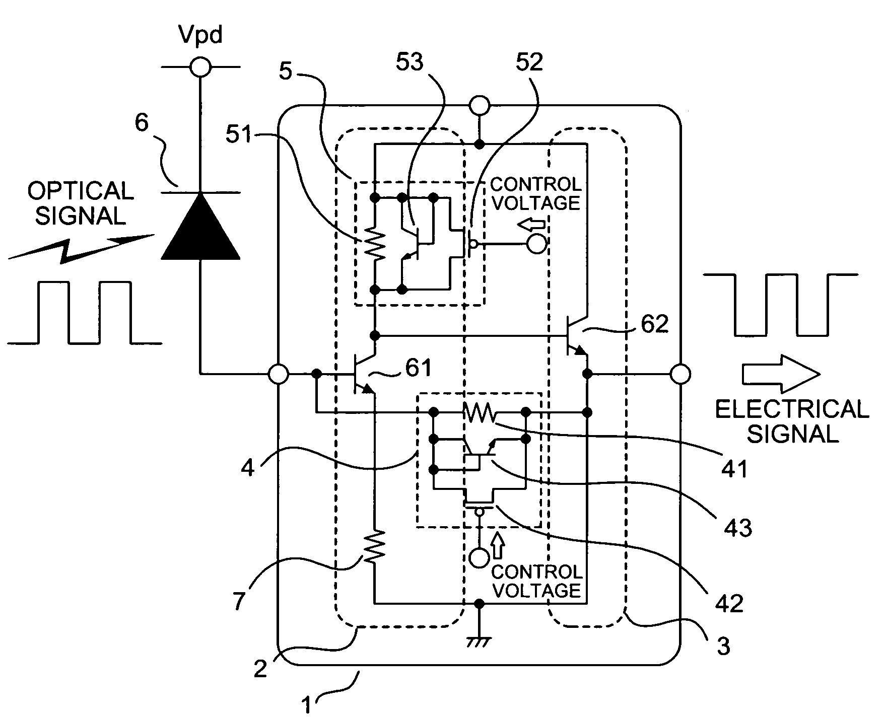
[0021]FIG. 1 is a diagram of a circuit configuration of a preamplifier according to the present invention. A preamplifier 1 of this figure includes an inverting amplifier circuit 2, an output buffer circuit 3, a feedback resistor portion 4, and a load resistor portion 5. The feedback resistor portion 4 includes a fixed resistor element 41, a MOSFET 42, and a diode-connected transistor 43, which are connected in parallel to one another. Likewise, the load resistor portion 5 includes a fixed resistor element 51, a MOSFET 52, and a diode-connected transistor 53, which are connected in parallel to one another. Further, connections are provided in these circuits as follows. That is, a base terminal of a transistor 62 that is an input terminal of the output buffer circuit 3 is connected to a collector terminal of a transistor 61 that is an output terminal of the inverting amplifier circuit 2. An emitter terminal of the transistor 62 that is an output terminal of the output buffer circuit ...
second embodiment
[0047]FIG. 5 is a diagram of a circuit configuration of a preamplifier according to the present invention. In this figure, portions the same as or equivalent to these in FIG. 1 are represented by the same signs. As shown in FIG. 5, a reference voltage Vref0 is supplied to the base terminal of the diode-connected transistor 53 that forms the load resistor portion 5. It is assumed that a collector terminal voltage of the transistor 61 provided in the inverting amplifier circuit 2 is defined as an input terminal voltage Vref1. Based on this, the reference voltage Vref0 becomes equivalent to the collector terminal voltage upon no signal input, that is, when the signal is not input to the inverting amplifier circuit 2.
[0048]Operation of the circuit as shown in FIG. 5 is explained below. If a current I1 flows into the feedback resistor portion 4 when an optical signal with a predetermined light intensity is received, the input terminal voltage Vref1 that is the collector terminal voltage ...
third embodiment
[0054]FIG. 6 is a diagram of a circuit configuration of a preamplifier according to the present invention. In this figure, portions the same as or equivalent to these in FIG. 1 are represented by the same signs. As shown in FIG. 6, a reference-bias-voltage generating circuit 8 includes a circuit equivalent to the preamplifier 1 of FIG. 1, i.e., the negative-feedback amplifier circuit. Further, a collector terminal of a transistor 81 that is an output terminal of the inverting amplifier circuit that forms the reference-bias-voltage generating circuit 8 is connected to the base terminal of the diode-connected transistor 53.
[0055]Operation of the circuit as shown in FIG. 6 is explained below. The reference-bias-voltage generating circuit 8 includes circuits equivalent to the basic components of the preamplifier 1 excluding the reference-bias-voltage generating circuit 8. Therefore, a voltage at the collector terminal of the transistor 81 that is an output terminal of the reference-bias...
PUM
 Abstract
Description
Claims
Application Information