
Off-width pitch for improved circuit card routing

a circuit card and off-width pitch technology, applied in the field of circuit card layout, can solve the problem that the general spacing requirements of the pcb are limited in the translation of the link, and achieve the effect of increasing the routing of the traces and enhancing the spacing

Active Publication Date: 2007-09-11
ALCATEL LUCENT SAS
View PDF11 Cites 20 Cited by
  • Summary
  • Abstract
  • Description
  • Claims
  • Application Information

AI Technical Summary

Benefits of technology

The invention provides a method for increasing the space available for routing traces in a ball grid array circuit card. This is achieved by modifying the spacing between rows or columns of vias in the land pattern of the circuit card. By translating the vias and their link connectors, additional routing areas can be created between the columns or rows. This results in a more efficient use of space, allowing for more traces to be routed through the circuit card. The method can be automated using a computer aided design program. The invention also provides a modified circuit card design with increased routing of traces through the vias.

Problems solved by technology

Via link translation is limited by general PCB spacing requirements.

Method used


Image

  • Off-width pitch for improved circuit card routing
  • Off-width pitch for improved circuit card routing
  • Off-width pitch for improved circuit card routing

Examples


Embodiment Construction

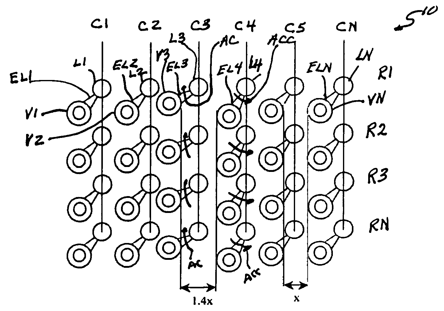
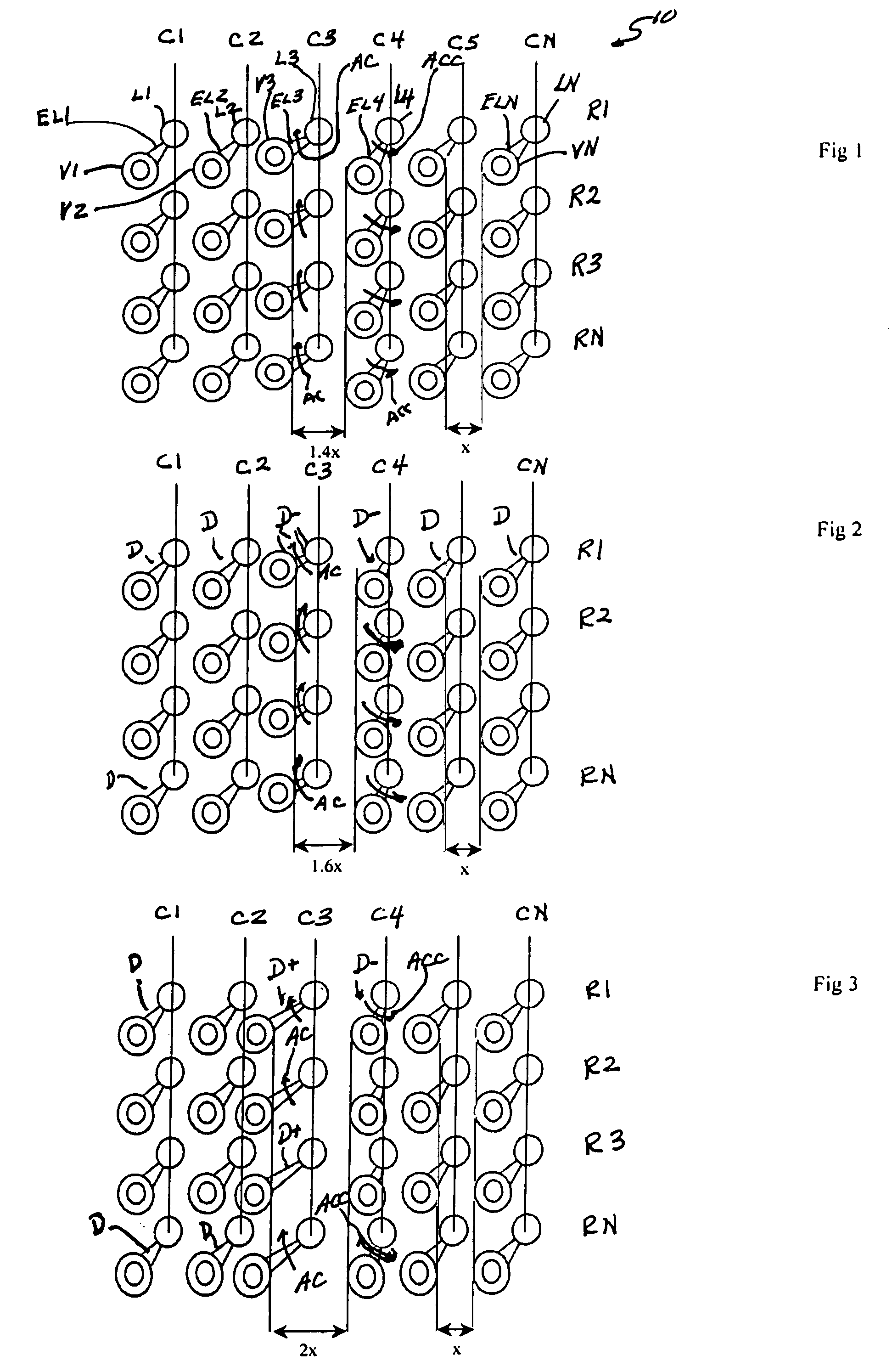
[0021]The invention addresses the problem of increasing the density of tracks routed through a grid of vias on a multi-layer circuit card, where the vias are arranged to accommodate interconnection requirements of a ball grid array (BGA) packaged device. Specifically, the need for this capability occurs when two or more tracks must be routed between adjacent rows (or columns) of vias in the grid, for example for edge coupled differential signals or simply to allow for localized high density escape. Currently, such routing is not possible on 1 mm pitch BGAs without compromising the via pad and / or via aspect ratio, which in turn can lead to manufacturing and reliability problems. The invention provides localized variances in the via pitch, thereby facilitating the 2 track routing scenario, while maintaining an average pitch that is equal to the pitch of the standard BGA package (e.g. 1 mm).

[0022]Referring to FIG. 1, a multilayered printed circuit board 10 having an array of columns C1...


PUM


Abstract

Enlarged spacing is provided between rows of vias in a ball grid array (BGA) multilayered printed wiring board land pattern in which the lands in the pattern are connected to the vias by a link connector by rotating, elongating, and / or truncating selected consecutive link connectors and rotating their respective corresponding vias in a row or column or selected consecutive rows or columns to achieve the enlarged spacing between rows or columns of vias in the BGA land pattern. Enhanced spacing between selected grid columns or rows of vias is provided such that some of the grid pitches for the vias are equal to that of the standard BGA and at least some are of a greater grid pitch.

Description

FIELD OF THE INVENTION[0001]The present invention relates to the layout of circuit cards and more specifically to routing signal traces within the array of a ball grid array (BGA), e.g. for high density escape, matched delay, or differential signal requirements.BACKGROUND AND BRIEF DESCRIPTION OF THE INVENTION[0002]1 mm pitch orthogonal BGAs currently represent the workhorse of most high complexity electronic designs. When these designs call for edge coupled differential signal traces to be routed from or through the pin fields of these 1 mm pitch BGA, space constraints and manufacturing limitations conspire to create a very challenging printed circuit board (PCB). When coupled with thicknesses in excess of 0.100″ (as is becoming routine), the capability to repeatably fabricate reliable product deteriorates rapidly. Challenges associated with this situation are well known in the industry.[0003]The problem is to provide a method of routing two or more traces through two rows of throu...

Claims


Application Information

Patent Timeline
Patent Type & Authority Patents(United States)
IPC IPC(8): G06F17/50H01L23/48
CPCH01L23/49827H01L23/49838H05K1/114H05K2201/09227H05K2201/094H01L2924/0002H05K2201/09418H05K2201/10734H01L2924/00
Inventor BROWN, PAUL
Owner ALCATEL LUCENT SAS
Learn More