Buffer circuit with current limiting
a buffer circuit and current limit technology, applied in logic circuits, pulse techniques, reliability increasing modifications, etc., can solve the problems of low output impedance provided by a given digital buffer circuit, reliability problems, and damage to the output stage devices themselves, so as to reduce the likelihood of damage and/or reliability problems.
- Summary
- Abstract
- Description
- Claims
- Application Information
AI Technical Summary
Benefits of technology
Problems solved by technology
Method used
Image

Examples
second embodiment
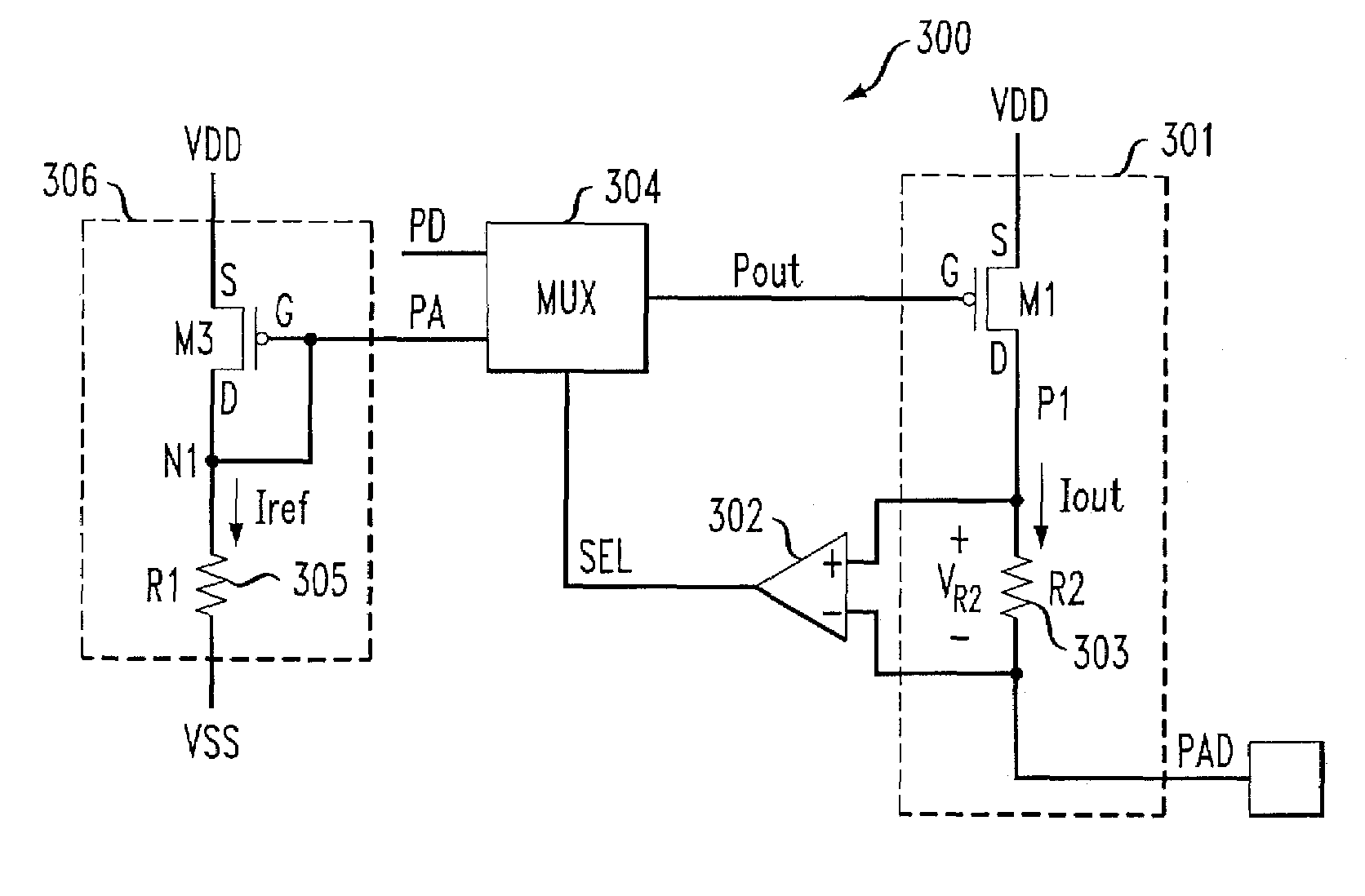
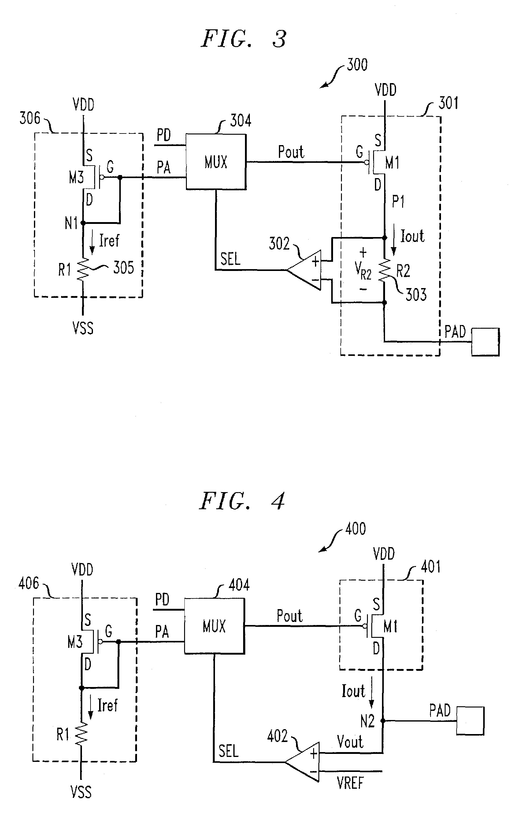
[0033]FIG. 4 is a schematic diagram depicting at least a portion of an exemplary buffer circuit 400, formed in accordance with the invention. The exemplary buffer circuit 400 comprises an output stage 401 connecting to an output pad (PAD) and generating an output current Iout, a comparator 402, or alternative detector circuit, and a multiplexer 404, or alternative control circuitry. The output stage 401 comprises a PMOS device M1 having a source terminal connecting to VDD, a drain terminal connected to the output pad at node N2, and a gate terminal connected to an output of the multiplexer 404. The multiplexer404 preferably includes a first input for receiving a digital signal PD, and a second input for receiving an analog signal PA. Analog signal PA may be generated by a bias source 406. The bias source 406 may comprise a diode-configured PMOS device M3 connected to VSS via a series resistor R1, although alternative bias circuits (e.g., bandgap reference, etc.) may be similarly emp...
third embodiment
[0037]FIG. 5 is a schematic diagram depicting at least a portion of an exemplary buffer circuit 500, formed in accordance with the invention. The exemplary buffer circuit 500 comprises an output stage 501 connectable to an output pad (PAD), first and second comparators 502 and 504, respectively, or alternative detection circuitry, and a multiplexer 506, or alternative control circuitry. The output stage 501 preferably includes a PMOS device M1 having a source terminal connecting to VDD, a drain terminal connected to the output pad at node N2, and a gate terminal connected to an output of the multiplexer 506. Alternative output stage arrangements are similarly contemplated by the invention. For example, although output stage 501 is depicted as including a single PMOS device M1 for sourcing current, it is to be understood that the output stage may further include an NMOS device (not shown) for sinking current, with the techniques of the present invention described herein similarly app...
PUM
 Abstract
Description
Claims
Application Information
 - R&D
- Intellectual Property
- Life Sciences
- Materials
- Tech Scout
- Unparalleled Data Quality
- Higher Quality Content
- 60% Fewer Hallucinations
Browse by: Latest US Patents, China's latest patents, Technical Efficacy Thesaurus, Application Domain, Technology Topic, Popular Technical Reports.
© 2025 PatSnap. All rights reserved.Legal|Privacy policy|Modern Slavery Act Transparency Statement|Sitemap|About US| Contact US: help@patsnap.com