
Borate phosphor materials for use in lighting applications

a technology of phosphor materials and lighting devices, which is applied in the direction of electroluminescent light sources, chemistry apparatuses and processes, and compositions of light sources, etc., can solve the problems that leds have not been suitable for lighting applications, and achieve high quantum efficiency and high cri

Inactive Publication Date: 2007-09-25
GELCORE LLC (US)
View PDF92 Cites 90 Cited by
  • Summary
  • Abstract
  • Description
  • Claims
  • Application Information

AI Technical Summary

Benefits of technology

These phosphor compositions enable the production of LEDs with higher quantum efficiency, greater color flexibility, and the ability to produce both colored and white light with enhanced CRI and lower CCTs, meeting the requirements for general illumination.

Problems solved by technology

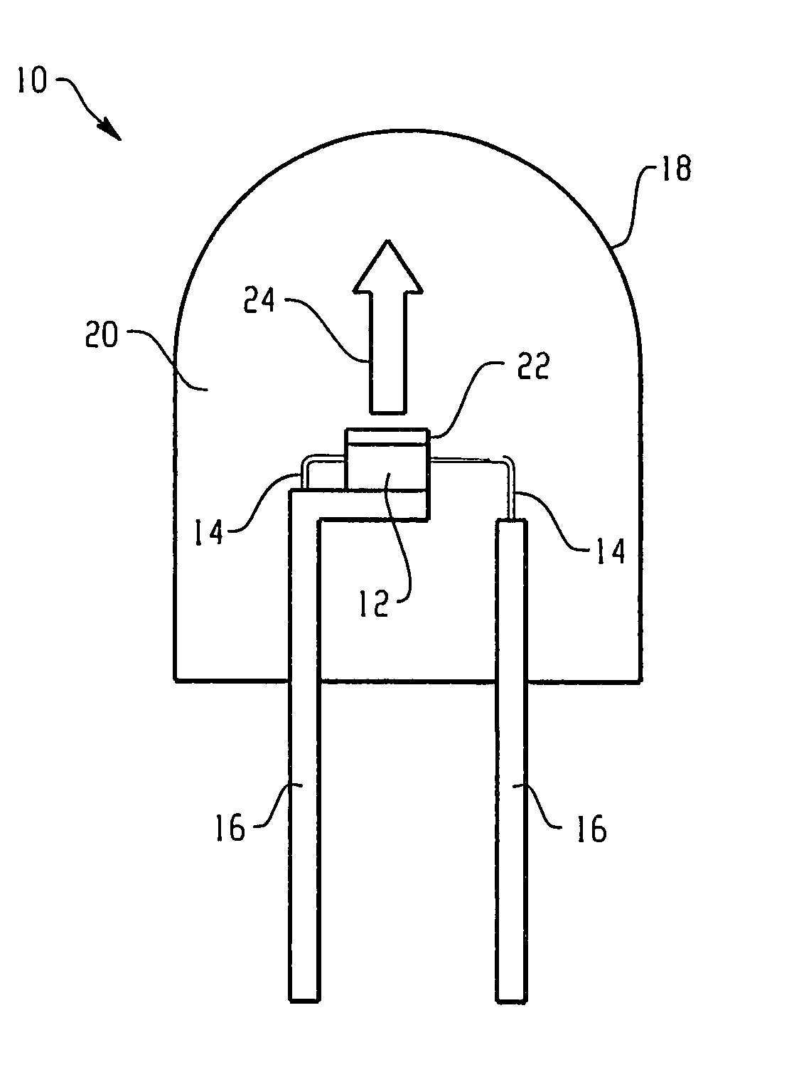
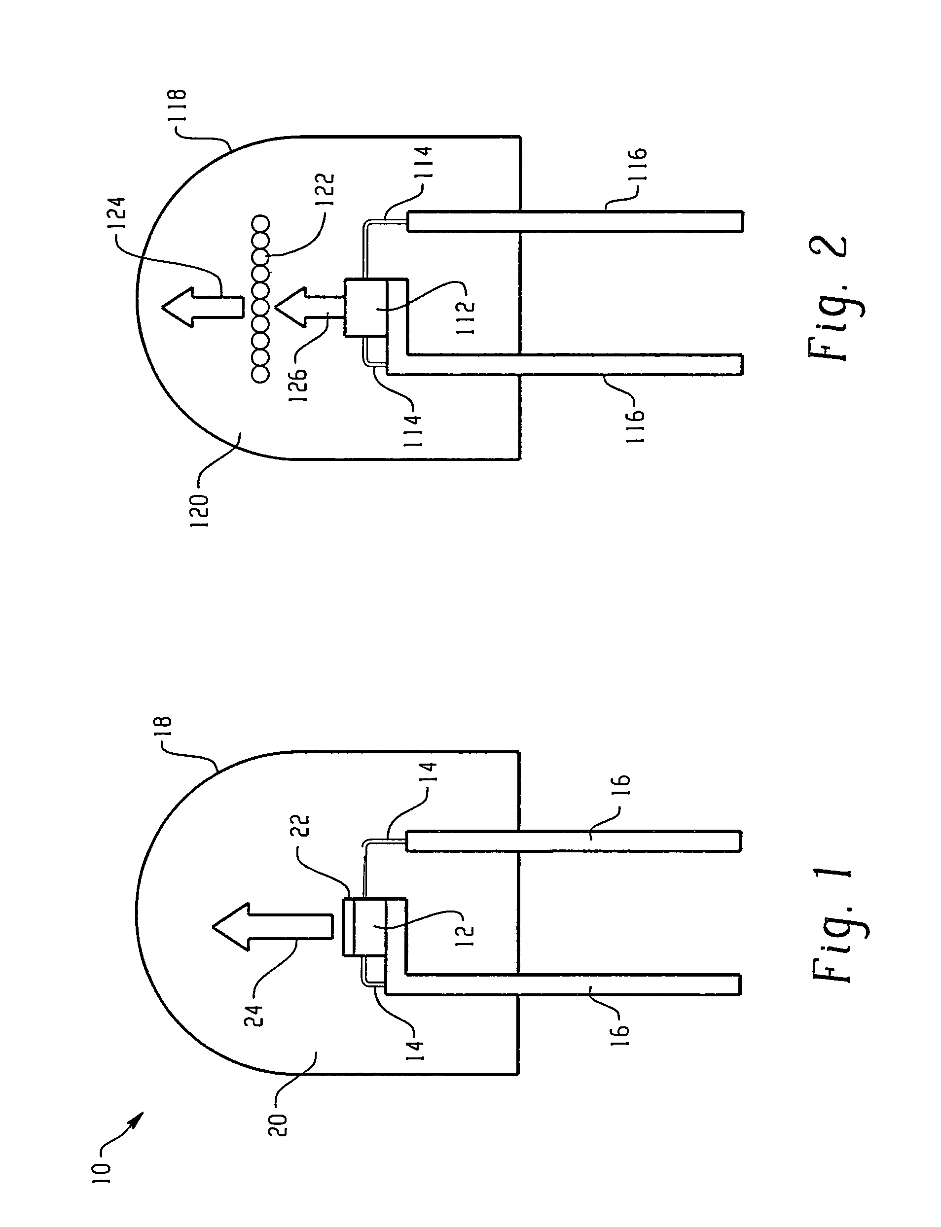
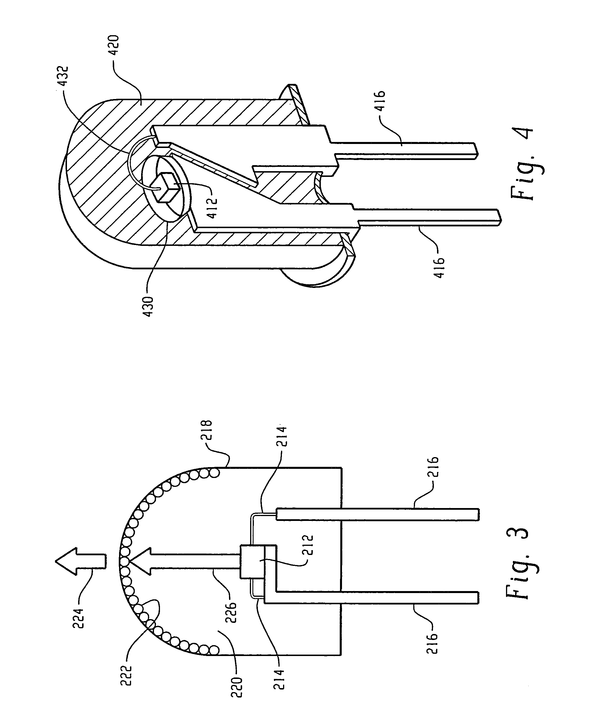
Until quite recently, LEDs have not been suitable for lighting uses where a bright white light is needed, due to the inherent color of the light produced by the LED.

Method used


Image

  • Borate phosphor materials for use in lighting applications
  • Borate phosphor materials for use in lighting applications
  • Borate phosphor materials for use in lighting applications

Examples


first embodiment

[0044]In a first embodiment, the phosphor composition includes a borate phosphor having the formula M3Ln2(BO3)4 doped with at least one activator selected from the group of Eu2+, Mn2+, Pb2+, Ce3+, Eu3+, Tb3+, and Bi3+ where M is at least one of Mg, Ca, Sr, Ba, or Zn, and Ln is at least one of Sc, Y, La, Gd, or Lu. In this embodiment, the LED chip preferably has a peak emission in the range of from 200-500 nm, more preferably from 220-410 nm. In the crystal arrangement, the divalent activators are thought to be situated at the site where M atoms would be while the trivalent activators take the place of Ln atoms. Thus, in the above formula, one or both of the M and Ln may be substituted with a dopant.

[0045]Exemplary compounds of this embodiment include: (Sr0.95Eu0.05)3Y2(BO3)4; Sr3(Y0.95Ce0.5)2(BO3)4; Sr3Y1.9Eu0.1(BO3)4; (Sr0.95Eu0.05)3Sc2(BO3)4; Sr3(Y0.45Sc0.5Ce0.05)2(BO3)4; Sr3Sc1.9Eu0.1(BO3)4; and (Ca0.95Mn0.05)3Y2(BO3)4.

[0046]FIGS. 5-11 are graphs showing the emission spectra of v...

second embodiment

[0047]In a second embodiment, the phosphor composition includes an oxide or oxynitride phosphor having the formula M′2−xM′x(Al, Ga)2−y(Si, Ge)yB2O7−zNz:Eu2+, Mn2+, Pb2+ where M′ is one or more of alkali metals Na and / or K, M″ is one or more of alkaline earth Mg, Ca, Sr, Ba or Zn, 0≦x≦2, 0≦y≦2, 0≦z≦4; and z=x+y. In this embodiment, the LED chip preferably has a peak emission in the range of from 200-500 nm, more preferably from 220-410 nm. Exemplary phosphors in this embodiment include Ca0.9NaAlSiB2O5N2:Mn2+; Sr0.9NaAlSi2B2O5N2:Eu2+; Ca0.9Si2B2O5N2:Mn2+; Sr0.9Si2B2O5N2:Eu2+ and Na2Si2B2O5N2.

[0048]FIGS. 12-15 are graphs showing the emission spectra of various phosphors according to the above second embodiment at an excitation wavelength of 405 nm. FIG. 12 is a graph showing the emission spectra of Ca0.9NaAlSi2B2O5N2:Mn2+. FIG. 13 is a graph showing the emission spectra of Sr0.9NaAlSiB2O5N2:Eu2+. FIG. 14 is a graph showing the emission spectra of Ca0.9Si2B2O5N2:Mn2+. FIG. 15 is a graph...

third embodiment

[0049]In a third embodiment, the phosphor composition comprises M′2−x+y′M″x−y′(Al, Ga)2−y(Si, Ge)yB2O7−z−y′NzXy:Eu2+, Mn2+, Pb2+ where M′ is one or more of alkali metals Na and / or K, M″ is one or more of alkaline earth metals Mg, Ca, Sr, Ba and / or Zn, 0≦x≦2, 0≦y≦2, 0≦z≦4; z=x+y, X═F and / or Cl, and 0≦y′≦2.


PUM


Abstract

Boron containing phosphor compositions having the formulas (1) M3Ln2(BO3)4 doped with at least one activator selected from the group of Eu2+, Mn2+, Pb2+, Ce3+, Eu3+, Tb3+, and Bi3+ where M is at least one of Mg, Ca, Sr, Ba, or Zn, and Ln is at least one of Sc, Y, La, Gd, or Lu; (2) M2−xM′x(Al, Ga)2−y(Si, Ge)yB2O7−zNz:Eu2+, Mn2+, Pb2+ where M′ is one or more of alkali metals Na and / or K, M″ is one or more of alkaline earth Mg, Ca, Sr, Ba or Zn, 0≦x≦2, 0≦y≦2, 0≦z≦4; and z=x+y; (3) M′2−x+y′M″x−y′(Al, Ga)2−y(Si, Ge)yB2O7−z−y′NzXy:Eu2+, Mn2+, Pb2+, where M′ is one or more of alkali metals Na and / or K, M″ is one or more of alkaline earth metals Mg, Ca, Sr, Ba and / or Zn, 0≦x≦2, 0≦y≦2, 0≦z≦4; z=x+y, X═F and / or Cl, and 0≦y′≦2; (4) M′2−xM″xAl2−y+y′Siy−y′B2O7−z−y′NzXy:Eu2+, Mn2+, Pb2+, where M′ and M″ are defined above, 0≦x≦2, 0≦y≦2, 0≦z≦4; z=x+y, X═F and / or Cl, and 0≦y′≦2; (5) M′2−x+x′M″x−x″Al2−y+y′Siy−y′B2O7−z−x′−y′NzX(x′+y′):Eu2+, Mn2+, Pb2+, where M′ and M″ are defined above, 0≦x≦2, 0≦y≦2, 0≦z≦4; z=x+y, X═F and / or Cl, and 0≦y′≦2; (6) MAl2B2O7:Eu2+, Mn2+, Pb2+; where M═Mg, Ca, Sr, Ba or Zn; (7) MAl2−xSixB2O7−xNx:Eu2+, Mn2+, Pb2+, where M═Mg, Ca, Sr, Ba and / or Zn, and 0≦x≦2; and (8) MAl2B2−xSixO7−xNx:Eu2+, Mn2+, Pb2+, where M═Mg, Ca, Sr, Ba and / or Zn, and 0≦x≦2. Also disclosed are light emitting devices including a light source and at least one of the above phosphor compositions.

Description

BACKGROUND[0001]The present exemplary embodiments relate to phosphor compositions and a lighting apparatus employing these compositions. It finds particular application in conjunction with light emitting diodes, and will be described with particular reference thereto. However, it is to be appreciated that the present exemplary embodiment is also amenable to other like applications.[0002]Light emitting diodes (LEDs) are semiconductor light emitters often used as a replacement for other light sources, such as incandescent lamps. They are particularly useful as display lights, warning lights and indicating lights or in other applications where colored light is desired. The color of light produce by an LED is dependent on the type of semiconducting material used in its manufacture.[0003]Colored semiconductor light emitting devices, including light emitting diodes and lasers (both are generally referred to herein as LEDs), have been produced from Group III-V alloys such as gallium nitrid...

Claims


Application Information

Patent Timeline
Patent Type & Authority Patents(United States)
IPC IPC(8): H01L33/00H01L33/50
CPCC09K11/0883C09K11/774H05B33/14H01L33/502H01L33/507H01L2924/181H01L2224/48091H01L2224/48247H01L2924/00012
Inventor CHANDRAN, RAMACHANDRAN GOPISHANKAR, MADRAS VENUGOPALSIVARAMAKRISHAN, VENKATRAMANSESHADRI, HARI NADATHUR
Owner GELCORE LLC (US)
Learn More