Supercharge Your Innovation With Domain-Expert AI Agents!

Semiconductor device and manufacturing method thereof

a technology of semiconductors and semiconductors, applied in the direction of semiconductor devices, electrical devices, transistors, etc., can solve problems such as and achieve the effect of suppressing the failure of a withstand voltag

Inactive Publication Date: 2007-10-02
SEMICON ENERGY LAB CO LTD +1
View PDF35 Cites 0 Cited by
  • Summary
  • Abstract
  • Description
  • Claims
  • Application Information

AI Technical Summary

Benefits of technology

[0010]In addition, in a manufacturing method of a semiconductor device according to the invention, after removal of the silicon oxide film by the solution, laser light or strong light is preferably irradiated to the crystalline semiconductor film. It enables not only to reduce crystal defects of the crystalline semiconductor film, but also to eliminate a shallow cavity.
[0048]Additionally, in a semiconductor device according to the invention, it is possible to form a gate insulating film so as to contact with the crystalline semiconductor film, form a gate electrode on the gate insulating film, and form source and drain regions in the crystalline semiconductor film. Since a TFT is formed by using such crystalline semiconductor film with production of a cavity suppressed, a defect of a withstand voltage can be suppressed.

Problems solved by technology

The cavity may cause some defect.
This cavity may remain even after irradiation of excimer laser light that is electromagnetic energy, and such crystalline silicon film having a cavity causes a defect of a withstand voltage in the case of forming a TFT or a capacitor in many cases.

Method used


Image

  • Semiconductor device and manufacturing method thereof
  • Semiconductor device and manufacturing method thereof
  • Semiconductor device and manufacturing method thereof

Examples


embodiment mode 1

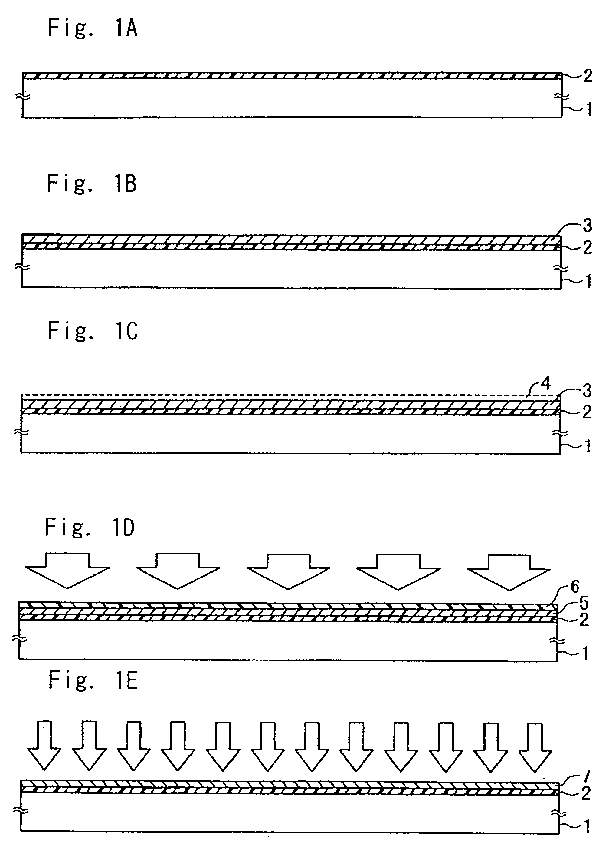
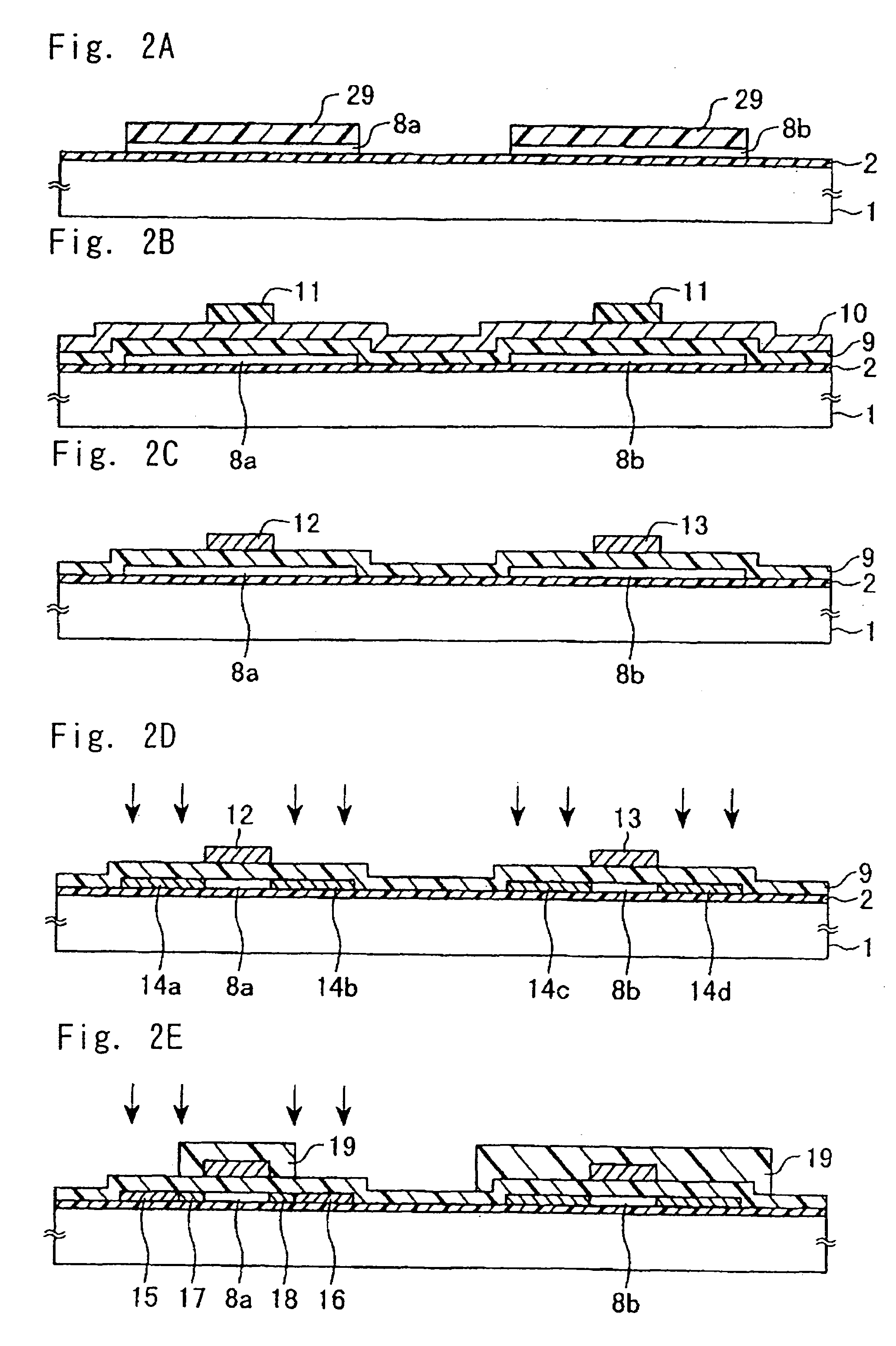
[0058]FIGS. 1A to 3D are cross-sectional views showing a manufacturing method of a semiconductor device according to Embodiment Mode 1 of the invention. A CMOS thin film transistor is cited as an example of the semiconductor device here.

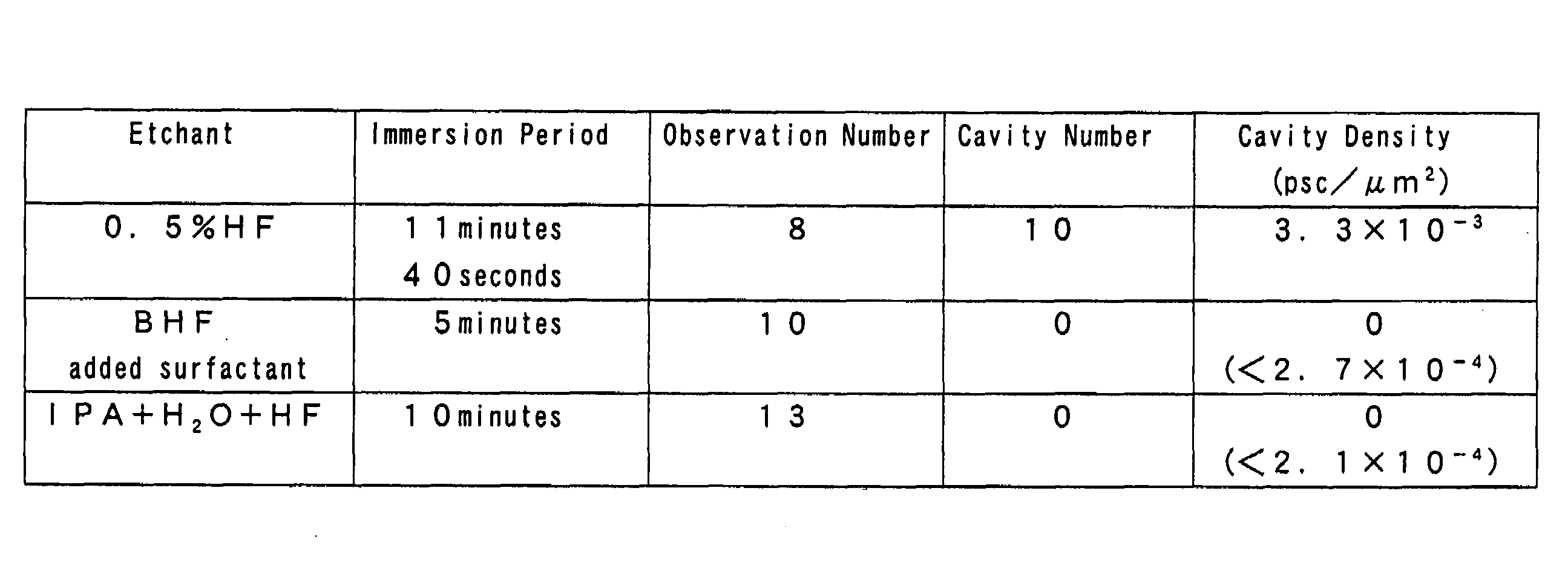
[0059]First, as illustrated in FIG. 1A, a base film is formed on a substrate 1, followed by a base insulating film 2 formed to have a thickness of approximately 100 nm.

[0060]The base insulating film 2 serves to prevent impurity diffusion from the substrate 1 to a semiconductor layer. A light transmissive substrate such as glass or quartz is employed for the substrate 1. In this embodiment mode, low alkali glass is employed for the substrate 1 and a silicon oxynitride film having a thickness of 100 nm formed by plasma CVD (chemical vapor deposition) is employed for the base insulating film 2.

[0061]Note that in this embodiment mode, although the base insulating film 2 has a single layer structure, a laminated structure of two or more layers may be adop...

embodiment mode 2

[0116]FIG. 4 is a cross-sectional view of a liquid crystal panel according to Embodiment Mode 2 of the invention. This liquid crystal panel is manufactured by the manufacturing method of a semiconductor device according to Embodiment Mode 1.

[0117]After a TFT array substrate 57 is formed in accordance with the manufacturing method of a semiconductor device according to Embodiment Mode 1, an alignment film 58 is formed in the TFT side of the TFT array substrate 57 and rubbing treatment is applied. The alignment film 58 comprises a polyimide resin or a polyamic-based resin.

[0118]A manufacturing method of an opposing substrate 59 is described below. A light shielding film 61 which is made of metal chromium is formed on a substrate 60. Then, a color filter 62 having three colors of red, blue, and green is provided on the light shielding film 61 arbitrarily. In the case where the color filter 62 is provided, a passivation film 63 which comprises an acrylic resin and the like is formed on ...


PUM

PropertyMeasurementUnit
areaaaaaaaaaaa
thicknessaaaaaaaaaa
thicknessaaaaaaaaaa

Abstract

A semiconductor device having a crystalline semiconductor film with production of a cavity suppressed and a manufacturing method thereof. A manufacturing method of a semiconductor device according to the invention comprises the steps of forming an amorphous silicon film on a substrate having an insulating surface, adding a metal element such as Ni for promoting crystallization to the amorphous silicon film, applying heat treatment to crystallize the amorphous silicon film, so that a crystalline silicon film is formed on the substrate, removing a silicon oxide film formed on the surface of the crystalline silicon film due to the heat treatment by a solution containing organic solvent and fluoride, and irradiating laser light or strong light to the crystalline silicon film.

Description

BACKGROUND OF THE INVENTION[0001]1. Field of the Invention[0002]The present invention relates to a semiconductor device and a manufacturing method thereof, and in particular, relates to a semiconductor device in which a cavity (a hole, an opening, a pore, and the like) is prevented from being produced at a crystalline semiconductor film and a manufacturing method thereof.[0003]2. Description of the Related Art[0004]When an amorphous silicon film is added with a metal such as Ni and heat treatment is applied thereto, a crystalline silicon film can be formed at low temperature in short time. Subsequently, a natural oxide film that is formed incidentally on the crystalline silicon film due to the heat treatment is removed by using diluted hydrofluoric acid. As the crystalline silicon film at this stage has many crystal defects, electromagnetic energy is supplied to the crystalline silicon film in the subsequent step. Consequently, a high-quality crystalline silicon film with few crysta...

Claims


Application Information

Patent Timeline
Patent Type & Authority Patents(United States)
IPC IPC(8): H01L21/84H01L29/786H01L21/20H01L21/336H01L21/77H01L27/12
CPCH01L27/1277H01L27/12H01L29/66757H01L21/02532H01L21/02667H01L21/02672H01L21/02686H01L21/2022H01L21/30604H01L21/3065H01L27/1214
Inventor OHNUMA, HIDETOSAKAKURA, MASAYUKIMITANI, YASUHIROMATSUO, TAKUYAKITAKADO, HIDEHITO
Owner SEMICON ENERGY LAB CO LTD
Features
  • R&D
  • Intellectual Property
  • Life Sciences
  • Materials
  • Tech Scout
  • Unparalleled Data Quality
  • Higher Quality Content
  • 60% Fewer Hallucinations
Learn More